HLMA-KL00 & HLMA-KH00 SunPower Series
T-1 (3 mm), High Performance AlInGaP LED Lamps
Data Sheet
Description
Features
These untinted, non-diffused, solid state lamps utilize
the latest absorbing substrate aluminum indium gallium
phosphide (AlInGaP) LED technology. These materials have
a very high luminous efficiency, capable of producing high
light output over a wide range of drive currents. In addition, these LED lamps are at wavelengths ranging from
amber to red orange.
• Outstanding LED Material Efficiency
• High Light Output over a Wide Range of Currents
• Low Electrical Power Dissipation
• Colors:
Amber
590 nm
Red-Orange
615 nm
Applications
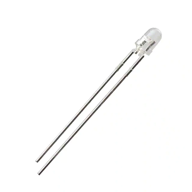
Package Dimensions
3.18 (0.125)
2.67 (0.105)
3.43 (0.135)
2.92 (0.115)
6.35 (0.250)
5.58 (0.220)
4.70 (0.185)
4.19 (0.165)
1.02 NOM.
(0.040)
24.10 MIN.
(0.95)
0.45 SQUARE
(0.018) NOMINAL
1.27
(0.050) NOM.
2.54 NOM.
(0.100)
CATHODE
NOTES:
1. ALL DIMENSIONS ARE IN MILLIMETERS (INCHES).
2. AN EPOXY MENISCUS MAY EXTEND ABOUT 0.8 MM (0.032")
DOWN THE LEADS, UNLESS OTHERWISE NOTED.
•
•
•
•
•
•
•
•
•
Outdoor Message Boards
Safety Lighting Equipment
Signaling Applications
Emitter for Emitter/Detector Applications
Changeable Message Signs
Portable Equipment
Medical Equipment
Automotive Lighting
Alternative to Incandescent Lamps
�Device Selection Guide
Dominant Wavelength
ld (nm) Typ
Luminous Intensity
Iv (mcd) at 20 mA-Min
Luminous Intensity
Iv (mcd) at 20 mA-Max
Amber
590nm
42.3
-
Red Orange
615nm
39.6
-
Part Number
Color
HLMA-KL00-I0000
HLMA-KH00-J0000
Tolerance for each intensity bin limit is ± 15%.
Absolute Maximum Ratings at TA = 25°C
Parameter
Value
Unit
DC Forward Current [1,4,5]
50
mA
Peak Forward Current [2]
200
mA
Time Average Input Power [2]
103
mW
Transient Forward Current [3] (10 ms Pulse)
500
mA
Reverse Voltage (IR = 100 mA)
5
V
Operating Temperature Range
-40 to 100
°C
Storage Temperature
-40 to 100
°C
Junction Temperature
110
°C
Notes:
1. Derate linearly as shown in Figure 4.
2. Any pulsed operation cannot exceed the Absolute Max Peak Forward Current or the Max Allowable Time Average Power as specified in Figure 5.
3. The transient peak current is the maximum nonrecurring peak current the device can withstand without damaging the LED die and wire bonds.
4. Drive Currents between 10 mA and 30 mA are recommended for best long term performance.
5. Operation at currents below 10 mA is not recommended, please contact your Avago Technologies sales representative.
Optical Characteristics at TA = 25°C
Part
Number
HLMA-
Luminous
Intensity
I (mcd) @ 20 mA [1]
Peak
Wavelength
l (nm)
Color, Dominant
Wavelength
l [2] (nm)
Viewing
Angle
2q½ Degrees [3]
Luminous
Flux (mlm)
@20 mA
Typ.
Min,
Typ.
Typ.
Min.
Max.
Typ.
Luminous
Efficacy
h(lm/w)
KL00
35
200
592
584.5
597.0
45
480
500
KH00
35
200
621
611.0
623.0
45
263
500
V
peak
d
v
Notes:
1. The luminous intensity, Iv, is measured at the mechanical axis of the lamp package. The actual peak of the spatial radiation pattern may not be
aligned with this axis.
2. The dominant wavelength, ?d, is derived from the CIE Chromaticity Diagram and represents the color of the device.
3. θ1/2 is the off-axis angle where the luminous intensity is 1/2 the peak intensity.
Electrical Characteristics at TA = 25°C
Reverse Breakdown
V (Volts)
@ I = 100 mA
Typ.
Max.
Min.
Typ.
Typ.
Thermal
Resistance
R (°C/W)
KL00
1.9
2.4
5
25
40
290
13
KH00
1.9
2.4
5
25
40
290
13
F
F
PART NUMBERHLMA-
2
R
R
Capacitance
C (pF) V = 0,
f = 1 MHz
Speed of Response (ns)
Time Constant
e-t/ts
Forward Voltage
V (Volts)
@ I = 20 mA
F
Ts
QJ-PIN
Typ.
�1.0
RELATIVE INTENSITY
AMBER
REDDISH-ORANGE
0.5
0
550
594 600
621 630
WAVELENGTH
650
700
Figure 1. Relative Intensity vs. Wavelength.
2.5
RELATIVE LUMINOUS INTENSITY
(NORMALIZED AT 20 mA)
1.5
2.0
2.5
V F - FORWARD VOLTAGE - V
IF - FORWARD CURRENT - mA
Figure 2. Forward Current vs. Forward Voltage, AS-AlInGaP.
50
45
40
35
30
25
20
15
10
5
0
RθJ-A = 618 °C/W
RθJ-A = 412 °C/W
0 10 20
30 40 0 60 70 80 90 100
T A - AMBIENT TEMPERATURE - °C
Figure 4. Maximum Forward Current vs. Ambient Temperature. Derating
Based on TJMAX = 110 °C.
3
2.0
1.5
1.0
0.5
0.0
3.0
0
10
20
30
40
IF - DC FORWARD CURRENT - mA
50
Figure 3. Relative Luminous Intensity vs. Forward Current.
IAVG - AVERAGE CURRENT - mA
IF - FORWARD CURRENT - mA
200
180
160
140
120
100
80
60
40
20
0
1.0
f ³ 1 KHz
50
40
30
f ³ 300 Hz
f ³ 100 Hz
20
10
0
50
150
100
IPEAK - PEAK FORWARD CURRENT - mA
Figure 5. Maximum Average Current vs. Peak Forward Current.
200
�1.0
0.9
NORMALIZED INTENSITY
0.8
0.7
0.6
0.5
0.4
0.3
0.2
0.1
0
100° 90° 80° 70° 60° 50° 40° 30° 20° 10° 0° 10° 20° 30° 40° 50° 60° 70° 80° 90° 100°
θ - ANGULAR DISPLACEMENT - (°)DEGREES
Figure 6. Normalized Luminous Intensity vs. Angular Displacement.
10
RELATIVE LOP
Red-orange
Amber
1
0.1
-50
-25
0
25
50
75
JUNCTION TEMPERATURE - °C
100
125
150
Figure 7. Relative light output vs. junction temperature
Amber Intensity Bin Limits (mcd at 20 mA)
Reddish-Orange Intensity Bin Limits (mcd at 20 mA)
Bin Name
Min.
Max.
Bin Name
Min.
Max.
I
42.3
67.7
J
39.6
63.4
J
67.7
108.2
K
63.4
101.5
K
108.2
173.2
L
101.5
162.4
L
173.2
250.0
M
162.4
234.6
M
250.0
360.0
N
234.6
340.0
N
360.0
510.0
O
340.0
540.0
O
510.0
800.0
P
540.0
850.0
P
800.0
1250.0
Q
850.0
1200.0
Q
1250.0
1800.0
Tolerance for each bin limit is ± 15%.
Tolerance for each bin limit is ± 15%.
Amber Color Bin Limits (nm at 20mA)
Bin Name
Min.
Max.
3
584.5
587.0
2
587.0
598.5
4
589.5
592.0
6
592.0
594.5
7
594.5
597.0
Tolerance for each bin limit is ± 0.5nm.
4
�Precautions:
Lead Forming:
• The leads of an LED lamp may be preformed or cut to
length prior to insertion and soldering on PC board.
• For better control, it is recommended to use proper
tool to precisely form and cut the leads to applicable
length rather than doing it manually.
• If manual lead cutting is necessary, cut the leads after
the soldering process. The solder connection forms a
mechanical ground which prevents mechanical stress
due to lead cutting from traveling into LED package.
This is highly recommended for hand solder operation,
as the excess lead length also acts as small heat sink.
Soldering and Handling:
• Care must be taken during PCB assembly and
soldering process to prevent damage to the LED
component.
• LED component may be effectively hand soldered to
PCB. However, it is only recommended under unavoidable circumstances such as rework. The closest manual
soldering distance of the soldering heat source
(soldering iron’s tip) to the body is 1.59mm. Soldering
the LED using soldering iron tip closer than 1.59mm
might damage the LED.
1.59mm
• ESD precaution must be properly applied on the
soldering station and personnel to prevent ESD
damage to the LED component that is ESD sensitive.
Do refer to Avago application note AN 1142 for details.
The soldering iron used should have grounded tip to
ensure electrostatic charge is properly grounded.
• Recommended soldering condition:
Wave
Soldering [1, 2]
Manual Solder
Dipping
Pre-heat temperature
105 °C Max.
-
Preheat time
60 sec Max
-
Peak temperature
250 °C Max.
260 °C Max.
Dwell time
3 sec Max.
5 sec Max
Note:
1. PCB with different size and design (component density) will have
different heat mass (heat capacity). This might cause a change in
temperature experienced by the board if same wave soldering setting is used. So, it is recommended to re-calibrate the soldering
profile again before loading a new type of PCB.
2. Avago Technologies’ high brightness LED are using high efficiency
LED die with single wire bond as shown below. Customer is advised
to take extra precaution during wave soldering to ensure that the
maximum wave temperature does not exceed 250°C and the solder
contact time does not exceeding 3sec. Over-stressing the LED during soldering process might cause premature failure to the LED due
to delamination.
Avago Technologies LED configuration
CATHODE
AlInGaP Device
• Any alignment fixture that is being applied during
wave soldering should be loosely fitted and should
not apply weight or force on LED. Non metal material
is recommended as it will absorb less heat during
wave soldering process.
• At elevated temperature, LED is more susceptible to
mechanical stress. Therefore, PCB must allowed to cool
down to room temperature prior to handling, which
includes removal of alignment fixture or pallet.
• If PCB board contains both through hole (TH) LED and
other surface mount components, it is recommended
that surface mount components be soldered on the
top side of the PCB. If surface mount need to be on the
bottom side, these components should be soldered
using reflow soldering prior to insertion the TH LED.
• Recommended PC board plated through holes (PTH)
size for LED component leads.
Note:
1) Above conditions refers to measurement with thermocouple
mounted at the bottom of PCB.
2) It is recommended to use only bottom preheaters in order to reduce
thermal stress experienced by LED.
• Wave soldering parameters must be set and maintained according to the recommended temperature and dwell time. Customer is advised to perform
daily check on the soldering profile to ensure that
it is always conforming to recommended soldering
conditions.
5
Note: Electrical connection between bottom surface of LED die and
the lead frame is achieved through conductive paste.
LED component
lead size
Diagonal
Plated through
hole diameter
0.45 x 0.45 mm
(0.018x 0.018 inch)
0.636 mm
(0.025 inch)
0.98 to 1.08 mm
(0.039 to 0.043 inch)
0.50 x 0.50 mm
(0.020x 0.020 inch)
0.707 mm
(0.028 inch)
1.05 to 1.15 mm
(0.041 to 0.045 inch)
• Over-sizing the PTH can lead to twisted LED after
clinching. On the other hand under sizing the PTH can
cause difficulty inserting the TH LED.
Refer to Application Note 5334 for more information about soldering and handling of high brightness TH LED lamps.
�Example of Wave Soldering Temperature Profile for TH LED
Recommended solder:
Sn63 (Leaded solder alloy)
SAC305 (Lead free solder alloy)
LAMINAR WAVE
HOT AIR KNIFE
TURBULENT WAVE
250
Flux: Rosin flux
Solder bath temperature:
245°C± 5°C (maximum peak
temperature = 250°C)
TEMPERATURE (°C)
200
Dwell time: 1.5 sec - 3.0 sec
(maximum = 3sec)
150
Note: Allow for board to be
sufficiently cooled to room
temperature before exerting
mechanical force.
100
50
PREHEAT
0
10
20
30
40
60
50
TIME (SECONDS)
70
80
90
Packaging Label
(i) Avago Mother Label: (Available on packaging box of ammo pack and shipping box)
(1P) Item: Part Number
STANDARD LABEL LS0002
RoHS Compliant
e3
max temp 250C
(1T) Lot: Lot Number
(Q) QTY: Quantity
LPN:
CAT: Intensity Bin
(9D)MFG Date: Manufacturing Date
BIN: Refer to below information
(P) Customer Item:
6
(V) Vendor ID:
(9D) Date Code: Date Code
DeptID:
Made In: Country of Origin
Lamps Baby Label
(1P) PART #: Part Number
(1T) LOT #: Lot Number
RoHS Compliant
e3
max temp 250C
100
�DeptID:
Made In: Country of Origin
(ii) Avago Baby Label (Only available on bulk packaging)
Lamps Baby Label
(1P) PART #: Part Number
RoHS Compliant
e3
max temp 250C
(1T) LOT #: Lot Number
(9D)MFG DATE: Manufacturing Date
QUANTITY: Packing Quantity
C/O: Country of Origin
Customer P/N:
CAT: Intensity Bin
Supplier Code:
BIN: Refer to below information
DATECODE: Date Code
Acronyms and Definition:
Example:
BIN:
(i) Color bin only or VF bin only
(Applicable for part number with color bins but
without VF bin OR part number with VF bins and no
color bin)
(i) Color bin only or VF bin only
BIN: 2 (represent color bin 2 only)
BIN: VB (represent VF bin “VB” only)
(ii) Color bin incorporate with VF Bin
BIN: 2VB
OR
(ii) Color bin incorporated with VF Bin
VB: VF bin “VB”
(Applicable for part number that have both color bin
and VF bin)
2: Color bin 2 only
DISCLAIMER: AVAGO’S PRODUCTS AND SOFTWARE ARE NOT SPECIFICALLY DESIGNED, MANUFACTURED
OR AUTHORIZED FOR SALE AS PARTS, COMPONENTS OR ASSEMBLIES FOR THE PLANNING, CONSTRUCTION,
MAINTENANCE OR DIRECT OPERATION OF A NUCLEAR FACILITY OR FOR USE IN MEDICAL DEVICES OR APPLICATIONS. CUSTOMER IS SOLELY RESPONSIBLE, AND WAIVES ALL RIGHTS TO MAKE CLAIMS AGAINST AVAGO
OR ITS SUPPLIERS, FOR ALL LOSS, DAMAGE, EXPENSE OR LIABILITY IN CONNECTION WITH SUCH USE.
For product information and a complete list of distributors, please go to our web site: www.avagotech.com
Avago, Avago Technologies, and the A logo are trademarks of Avago Technologies in the United States and other countries.
Data subject to change. Copyright © 2005-2014 Avago Technologies. All rights reserved. Obsoletes AV02-0648EN
AV02-1524EN - July 21, 2014
�
很抱歉,暂时无法提供与“HLMA-KL00-I0000”相匹配的价格&库存,您可以联系我们找货
免费人工找货- 国内价格 香港价格
- 1+8.827181+1.14343