HLMP-331x, HLMP-341x, HLMP-351x Series
T-13/4 (5 mm) High Intensity LED Lamps
Data Sheet
Description
Features
This family of T-13/4 nondiffused LED lamps is
specially designed for applica
tions requiring higher
on-axis intensity than is achievable with a standard
lamp. The light generated is focused to a narrow
beam to achieve this effect.
• High intensity
• Choice of 3 bright colors
- High Efficiency Red
- Yellow
- High Performance Green
Selection Guide
Luminous Intensity Iv (mcd) @ 10 mA
• Popular T-13/4 diameter package
• Selected minimum intensities
Color
Part Number
Min.
Max.
Red
HLMP-3316
24.8
-
HLMP-3316-I00xx
24.8
-
• General purpose leads
Yellow
HLMP-3416
16.6
-
• Reliable and rugged
Green
HLMP-3519
12.0
-
• Available on tape and reel
HLMP-3519-F00xx
12.0
-
• Narrow viewing angle
�Part Numbering System
HLMP - 3 x 1 x - x x x xx
Mechanical Options
00: Bulk
01: Tape & Reel, Crimped Leads
02: Tape & Reel, Straight Leads
B1: Right Angle Housing, Uneven Leads
B2: Right Angle Housing, Even Leads
Color Bin Options
0: Full Color Bin Distribution
Maximum Iv Bin Options
0: Open (no max. limit)
Others: Please refer to the Iv Bin Table
Minimum Iv Bin Options
Please refer to the Iv Bin Table
Brightness Level
6, 9: Higher Brightness
Color Options
3: GaP HER
4: GaP Yellow
5: GaP Green
Package Dimensions
5.08 (0.200)
4.57 (0.180)
9.19 (0.362)
8.43 (0.332)
0.65 MAX.
(0.026)
0.89 (0.035)
0.64 (0.025)
25.40
(1.00) MIN.
CATHODE
LEAD
(NOTE 1)
1.27 (0.050)
NOM.
0.46 (0.018)
SQUARE
NOM.
6.10 (0.240)
5.59 (0.220)
2.54 (0.100)
NOM.
2
Notes:
1. All dimensions are in millimeters (inches).
2. An epoxy meniscus may extend about 1 mm (0.40") down the leads.
3. For PCB hole recommendations, see the Precautions section.
�Electrical Characteristics at TA = 25°C
Symbol
Description
Device
HLMP-
Min.
Typ.
IV
3316
24.8
60.0
3416
3519
2q1/2
Luminous Intensity
Max.
Units
Test Conditions
mcd
IF = 10 mA (Figure 3)
16.6 50.0
mcd
IF = 10 mA (Figure 8)
12.0 70.0
mcd
IF = 10 mA (Figure 13)
Including Angle Between Half
3316
35
Deg.
Luminous Intensity Points
IF = 10 mA
See Note 1 (Figure 6)
3416
35 Deg. IF = 10 mA
See Note 1 (Figure 11)
3519
24 Deg. IF = 10 mA
See Note 1 (Figure 16)
lPEAK
Peak Wavelength
331X
635
nm
Measurement at Peak
341X 583 (Figure 1)
351X 565
Dl1/2
Spectral Line Halfwidth
331X
341X
351X
40
36
28
nm
ld
Dominant Wavelength
331X
341X
351X
626
585
569
nm
ts
Speed of Response
331X
341X
351X
90
90
500
ns
C
Capacitance
331X
341X
351X
11
15
18
pF
RqJ-PIN
Thermal Resistance
331X
260
°C/W
Junction to Cathode
341X Lead
351X
VF
Forward Voltage
331X
1.9
2.4
V
IF = 10 mA (Figure 2)
341X 2.0
2.4 IF = 10 mA (Figure 7)
351X 2.1
2.7 IF = 10 mA (Figure 12)
VR
All
Reverse Breakdown Volt.
hV
Luminous Efficacy
5.0
331X
341X
351X
V
145
lumens
500 Watt
595
See Note 2 (Figure 1)
VF = 0; f = 1 MHz
IR = 100 µA
See Note 3
Notes:
1. q1/2 is the off-axis angle at which the luminous intensity is half the axial luminous intensity.
2. The dominant wavelength, ld, is derived from the CIE chromaticity diagram and represents the single wavelength which defines the color of
the device.
3. Radiant intensity, Ie, in watts/steradian, may be found from the equation Ie = Iv/hv, where Iv is the luminous intensity in candelas and hv is the
luminous efficacy in lumens/watt.
3
�Absolute Maximum Ratings at TA = 25°C
Parameter
331X Series
341X Series
351X Series
Units
Peak Forward Current
90
60
90
mA
20
25
mA
Average Forward Current[1] 25
DC Current[2]
30 20 30
mA
Power Dissipation[3]
135 85 135
mW
Reverse Voltage (IR = 100 µA)
5
5
5
V
Transient Forward Current[4] 500
(10 µsec Pulse)
500
500
mA
LED Junction Temperature
110
110
110
°C
Operating Temperature Range
-40 to +100
-40 to +100
-20 to +100
°C
Storage Temperature Range
-40 to +100
-40 to +100
-40 to +100
°C
Notes:
1. See Figure 5 (Red), 10 (Yellow), or 15 (Green) to establish pulsed operating conditions.
2. For Red and Green series derate linearly from 50°C at 0.5 mA/°C. For Yellow series derate linearly from 50°C at 0.2 mA/°C.
3. For Red and Green series derate power linearly from 25°C at 1.8 mW/°C. For Yellow series derate power linearly from 50°C at 1.6 mW/°C.
4. The transient peak current is the maximum non-recurring peak current that can be applied to the device without damaging the LED die and
wirebond. It is not recommended that the device be operated at peak currents beyond the peak forward current listed in the Absolute Maximum Ratings.
Figure 1. Relative intensity vs. wavelength.
4
�High Efficiency Red HLMP-331X Series
Figure 2. Forward current vs. forward voltage
characteristics.
Figure 5. Maximum tolerable peak current vs.
pulse duration (IDC MAX as per MAX ratings).
5
Figure 3. Relative luminous intensity vs. DC
forward current.
Figure 4. Relative efficiency (luminous intensity
per unit current) vs. peak LED current.
Figure 6. Relative luminous intensity vs. angular displacement.
�Yellow HLMP-341X Series
Figure 7. Forward current vs. forward voltage
characteristics.
Figure 10. Maximum tolerable peak current vs.
pulse duration (IDC MAX as per MAX ratings).
6
Figure 8. Relative luminous intensity vs. DC
forward current.
Figure 9. Relative efficiency (luminous intensity
per unit current) vs. peak current.
Figure 11. Relative luminous intensity vs. angular displacement.
�Green HLMP-351X Series
Figure 12. Forward current vs. forward voltage
characteristics.
Figure 15. Maximum tolerable peak current vs.
pulse duration (IDC MAX as per MAX ratings).
7
Figure 13. Relative luminous intensity vs. DC
forward current.
Figure 14. Relative efficiency (luminous intensity per unit current) vs. peak LED current.
Figure 16. Relative luminous intensity vs. angular displacement. T-13/4 lamp.
�Table 2. Intensity Bin Limit
Table 2. (Cont'd)
Table 2. (Cont'd)
Intensity Range
(mcd)
Intensity Range
(mcd)
Intensity Range
(mcd)
Color
Bin
Color
Bin
Color
Bin
H 15.5 24.8
G 16.6 26.5
E 7.6
I 24.8 39.6
H 26.5 42.3
F 12.0 19.1
J 39.6 63.4
I 42.3 67.7
G 19.1 30.7
K 63.4 101.5
J 67.7 108.2
H 30.7 49.1
L 101.5 162.4
K 108.2 173.2
I 49.1 78.5
M 162.4 234.6
L 173.2 250.0
J 78.5 125.7
N 234.6 340.0
M 250.0 360.0
K 125.7 201.1
O 340.0 540.0
Yellow N 360.0
L 201.1 289.0
Min.
Max.
Min.
Max.
510.0
Min.
Max.
12.0
Red P 540.0 850.0
O 510.0 800.0
Green M 289.0 417.0
Q 850.0 1200.0
P 800.0 1250.0
N 417.0 680.0
R 1200.0 1700.0
Q 1250.0 1800.0
O 680.0 1100.0
S 1700.0 2400.0
R 1800.0 2900.0
P 1100.0 1800.0
T 2400.0 3400.0
S 2900.0 4700.0
Q 1800.0 2700.0
U 3400.0 4900.0
T 4700.0 7200.0
R 2700.0 4300.0
V 4900.0 7100.0
U 7200.0 11700.0
S 4300.0 6800.0
W 7100.0 10200.0
V 11700.0 18000.0
T 6800.0 10800.0
X 10200.0 14800.0
W 18000.0 27000.0
U 10800.0 16000.0
Y 14800.0 21400.0
V 16000.0 25000.0
Z 21400.0 30900.0
W 25000.0 40000.0
Maximum tolerance for each bin limit is ±18%.
8
�Color Categories
Lambda (nm)
Color
Cat #
Min.
6
561.5 564.5
Max.
5
564.5 567.5
Green 4
567.5 570.5
3
570.5 573.5
2
573.5 576.5
1
582.0 584.5
3
584.5 587.0
Yellow 2
587.0 589.5
4
589.5 592.0
5
592.0 593.0
Tolerance for each bin limit is ± 0.5 nm.
Mechanical Option Matrix
Mechanical Option Code
Definition
00
Bulk Packaging, minimum increment 500 pcs/bag
01
Tape & Reel, crimped leads, minimum increment 1300 pcs/bag
02
Tape & Reel, straight leads, minimum increment 1300 pcs/bag
B1
Right Angle Housing, uneven leads, minimum increment 500 pcs/bag
B2
Right Angle Housing, even leads, minimum increment 500 pcs/bag
Note:
All Categories are established for classification of products. Products may not be available in all categories. Please contact your local Avago representative for further clarification/information.
9
�Precautions
Lead Forming
• The leads of an LED lamp may be preformed or cut to
length prior to insertion and soldering into PC board.
• If lead forming is required before soldering, care must
be taken to avoid any excessive mechanical stress
induced to LED package. Otherwise, cut the leads
of LED to length after soldering process at room
temperature. The solder joint formed will absorb the
mechanical stress of the lead cutting from traveling to
the LED chip die attach and wirebond.
• It is recommended that tooling made to precisely
form and cut the leads to length rather than rely upon
hand operation.
Soldering Conditions
• Care must be taken during PCB assembly and soldering
process to prevent damage to LED component.
• The closest LED is allowed to solder on board is 1.59
mm below the body (encapsulant epoxy) for those
parts without standoff.
• Wave soldering parameter must be set and maintained
according to recommended temperature and dwell
time in the solder wave. Customer is advised to
periodically check on the soldering profile to ensure
the soldering profile used is always conforming to
recommended soldering condition.
• If necessary, use fixture to hold the LED component
in proper orientation with respect to the PCB during
soldering process.
• Proper handling is imperative to avoid excessive
thermal stresses to LED components when heated.
Therefore, the soldered PCB must be allowed to cool
to room temperature, 25°C, before handling.
• Special attention must be given to board fabrication,
solder masking, surface plating and lead holes size
and component orientation to assure solderability.
• Recommended PC board plated through hole sizes
for LED component leads:
• Recommended soldering conditions:
Diagonal
Plated Through
-Hole Diameter
0.98 to 1.08 mm
(0.039 to 0.043 in)
Wave Soldering
Manual Solder
Dipping
Lead size (typ.)
0.45 × 0.45 mm
(0.018 × 0.018 in.)
0.636 mm
(0.025 in)
Pre-heat Temperature
105 °C Max.
–
Pre-heat Time
30 sec Max.
–
Dambar shearoff area (max.)
0.65 mm
(0.026 in)
0.919 mm
(0.036 in)
Peak Temperature
250 °C Max.
260 °C Max.
Lead size (typ.)
Dwell Time
3 sec Max.
5 sec Max.
0.50 × 0.50 mm
(0.020 × 0.020 in.)
0.707 mm
(0.028 in)
Dambar shearoff area (max.)
0.70 mm
(0.028 in)
0.99 mm
(0.039 in)
TURBULENT WAVE
250
TEMPERATURE – °C
LED Component
Lead Size
LAMINAR WAVE
HOT AIR KNIFE
FLUXING
100
PREHEAT
0
10
20
30
on soldering LED components.
CONVEYOR SPEED = 1.83 M/MIN (6 FT/MIN)
PREHEAT SETTING = 150°C (100°C PCB)
SOLDER WAVE TEMPERATURE = 245°C
AIR KNIFE AIR TEMPERATURE = 390°C
AIR KNIFE DISTANCE = 1.91 mm (0.25 IN.)
AIR KNIFE ANGLE = 40
SOLDER: SN63; FLUX: RMA
150
50
30
Note: Refer to application note AN1027 for more information
BOTTOM SIDE
OF PC BOARD
TOP SIDE OF
PC BOARD
200
40
50
60
TIME – SECONDS
70
80
90
100
NOTE: ALLOW FOR BOARDS TO BE
SUFFICIENTLY COOLED BEFORE EXERTING
MECHANICAL FORCE.
Figure 17. Recommended wave soldering profile.
For product information and a complete list of distributors, please go to our website:
1.05 to 1.15 mm
(0.041 to 0.045 in)
www.avagotech.com
Avago, Avago Technologies, and the A logo are trademarks of Avago Technologies in the United States and other countries.
Data subject to change. Copyright © 2005-2015 Avago Technologies. All rights reserved. Obsoletes 5989-4259EN
AV02-1023EN - April 15, 2015
�
很抱歉,暂时无法提供与“HLMP-3416”相匹配的价格&库存,您可以联系我们找货
免费人工找货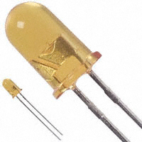


 工商网监
湘ICP备2023018690号
工商网监
湘ICP备2023018690号
