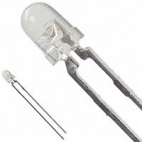
HLMP-D101/D105, HLMP-K101/K105
T-13/4 (5 mm), T-1 (3 mm), High Intensity,
Double Heterojunction AlGaAs Red LED Lamps
Data Sheet
Description
Features
These solid-state LED lamps utilize newly developed
double heterojunction (DH) AlGaAs/GaAs material technology. This LED material has outstanding light output
efficiency over a wide range of drive currents. The color is
deep red at the dominant wavelength of 637 nanometers.
These lamps may be DC or pulse driven to achieve desired
light output.
• Exceptional brightness
• Wide viewing angle
• Outstanding material efficiency
• Low forward voltage
• CMOS/MOS compatible
• TTL compatible
• Deep red color
Applications
• Bright ambient lighting conditions
• Moving message panels
• Portable equipment
• General use
Package Dimensions
6.10 (0.240)
5.59 (0.220)
0.89 (0.035)
0.64 (0.025)
0.65 (0.026) max
0.40 (0.016)
CATHODE LEAD
9.19 (0.362)
8.43 (0.332)
25.40(1.00)
MINIMUM
1.27(0.050)
NOM.
A
1.14 (.045)
0.51 (.020)
3.43 (.135)
2.92 (.115)
Ø
0.89 (0.035)
0.64 (0.025)
13.25 (0.522)
12.45 (0.490)
5.08 (0.200)
4.57 (0.180)
2.54 (0.100) NOM.
5.08 (0.200)
4.57 (0.180)
SQUARE TYP.
0.55 (0.022)
1.32 (0.052)
1.02 (0.040)
23.0
MIN.
(0.90)
0.46 (0.018)
SQUARE NOMINAL
2.79 (.110)
2.29 (.090)
24.1(.95) MIN.
0.65 (0.026) max.
1.52 (.060)
1.02 (.040)
1.27 (0.050)
NOM.
3.17 (.125)
2.67 (.105)
6.1 (0.240)
5.6 (0.220)
(0.022) 0.55 SQ. TYP.
(0.016) 0.40
4.70 (.185)
4.19 (.165)
9.19 (0.362)
8.43 (0.332)
CATHODE
2.54 (0.100)
NOM.
6.35 (.250)
5.58 (.220)
B
C
Notes:
1. All dimensions are in mm (inches).
2. An epoxy meniscus may extend about 1 mm (0.040") down the leads.
3. For PCB hole recommendations, see the Precautions section.
�Selection Guide
Luminous Intensity Iv (mcd) at 20 mA
Package Description
Device HLMP-
Min.
Typ.
Max.
2θ1/2[1]
Degree
T-1 3/4 Red Tinted Diffused
D101
35.2
70.0
–
65
A
D101-J00xx
35.2
70.0
–
65
A
D101-JK0xx
35.2
70.0
112.8
65
A
D105
138.0
240.0
–
24
B
D105-M00xx
138.0
240.0
–
24
B
K101
22.0
45.0
–
60
C
K101-I00xx
22.0
45.0
–
60
C
K105
35.2
65.0
–
45
C
K105-J00xx
35.2
65.0
–
45
C
T-1 3/4 Red Untinted Non-diffused
T-1 Red Tinted Diffused
T-1 Red Untinted Non-diffused
Note:
1. θ1/2 is the off axis angle from lamp centerline where the luminous intensity is 1/2 the on-axis value.
Part Numbering System
HLMP - x x xx - x x x xx
Mechanical Option
00: Bulk
02: Tape & Reel, Straight Leads
Color Bin Options
0: Full Color Bin Distribution
Maximum Iv Bin Options
0: Open (no max. limit)
Others: Please refer to the Iv Bin Table
Minimum Iv Bin Options
Please refer to the Iv Bin Table
Lens Type
01: Tinted, Diffused
05: Untinted, Nondiffused
Color Options
1: AlGaAs Red
Package Options
D: T-13/4
K: T-1
2
Package
Outline
�Absolute Maximum Ratings at TA = 25°C
Parameter
Value
Peak Forward Current[1,2]
300 mA
Average Forward Current[2]
20 mA
DC Current[3]
30 mA
Power Dissipation
87 mW
Reverse Voltage (IR = 100 μA)
5V
Transient Forward Current (10 μs Pulse)[4]
500 mA
LED Junction Temperature
110°C
Operating Temperature Range
-20 to +100°C
Storage Temperature Range
-40 to +100°C
Notes:
1. Maximum IPEAK at f = 1 kHz, DF = 6.7%.
2. Refer to Figure 6 to establish pulsed operating conditions.
3. Derate linearly as shown in Figure 5.
4. The transient peak current is the maximum non-recurring peak current the device can withstand without damaging the LED die and wire bonds.
It is not recommended that the device be operated at peak currents beyond the Absolute Maximum Peak Forward Current.
Electrical/Optical Characteristics at TA = 25°C
Symbol
Description
VF
Forward Voltage
VR
Reverse Breakdown Voltage
λp
Min.
Typ.
Max.
Unit
Test Condition
1.8
2.2
V
IF = 20 mA
15.0
V
IR = 100 μA
Peak Wavelength
645
nm
Measurement at Peak
λd
Dominant Wavelength
637
nm
Note 1
Δλ1/2
Spectral Line Halfwidth
20
nm
τS
Speed of Response
30
ns
Exponential Time
Constant, e-t/TS
C
Capacitance
30
pF
VF = 0, f = 1 MHz
RθJ-PIN
Thermal Resistance
260[3]
210[4]
290[5]
°C/W
Junction to Cathode
Lead
ηV
Luminous Efficacy
80
Im/W
Note 2
5.0
Notes:
1. The dominant wavelength, λd, is derived from the CIE chromaticity diagram and represents the color of the device.
2. The radiant intensity, Ie, in watts per steradian, may be found from the equation Ie = lV/ηV, where IV is the luminous intensity in candelas and ηV is
luminous efficacy in lumens/watt.
3. HLMP-D101.
4. HLMP-D105.
5. HLMP-K101/-K105.
3
�Figure 1. Relative intensity vs. wavelength.
Figure 2. Forward current vs. forward voltage.
Figure 3. Relative luminous intensity vs. dc forward current.
Figure 4. Relative efficiency vs. peak forward current.
Figure 5. Maximum forward dc current vs. ambient temperature.
Derating based on TJ MAX. = 110°C.
Figure 6. Maximum tolerable peak current vs. peak duration
(IPEAK MAX. determined from temperature derated IDC MAX.).
4
�Figure 7. Relative luminous intensity vs. angular displacement. HLMP-D101.
Figure 8. Relative luminous intensity vs. angular displacement. HLMP-K101.
Figure 9. Relative luminous intensity vs. angular displacement. HLMP-D105.
Figure 10. Relative luminous intensity vs. angular displacement. HLMP-K105.
5
�Intensity Bin Limits
Intensity Range (mcd)
Color
Bin
Min.
Max.
Red
I
24.8
39.6
J
39.6
63.4
K
63.4
101.5
L
101.5
162.4
M
162.4
234.6
N
234.6
340.0
O
340.0
540.0
P
540.0
850.0
Q
850.0
1200.0
R
1200.0
1700.0
S
1700.0
2400.0
T
2400.0
3400.0
U
3400.0
4900.0
V
4900.0
7100.0
W
7100.0
10200.0
X
10200.0
14800.0
Y
14800.0
21400.0
Z
21400.0
30900.0
Maximum tolerance for each bin limit is ± 18%.
Mechanical Option Matrix
Mechanical Option Code
Definition
00
Bulk Packaging, minimum increment 500 pcs/bag
02
Tape & Reel, straight leads, minimum increment 1300 pcs (T-13/4)/1800 pcs (T-1)
Note:
All categories are established for classification of products. Products may not be available in all categories. Please contact your local Avago representative
for further clarification/information.
6
�Precautions
Lead Forming:
• The leads of an LED lamp may be preformed or cut to
length prior to insertion and soldering on PC board.
• For better control, it is recommended to use proper
tool to precisely form and cut the leads to applicable
length rather than doing it manually.
• If manual lead cutting is necessary, cut the leads after
the soldering process. The solder connection forms a
mechanical ground which prevents mechanical stress
due to lead cutting from traveling into LED package.
This is highly recommended for hand solder operation,
as the excess lead length also acts as small heat sink.
Soldering and Handling:
• Care must be taken during PCB assembly and soldering
process to prevent damage to the LED component.
• LED component may be effectively hand soldered
to PCB. However, it is only recommended under
unavoidable circumstances such as rework. The closest
manual soldering distance of the soldering heat source
(soldering iron’s tip) to the body is 1.59mm. Soldering
the LED using soldering iron tip closer than 1.59mm
might damage the LED.
1.59 mm
• ESD precaution must be properly applied on the
soldering station and personnel to prevent ESD
damage to the LED component that is ESD sensitive.
Do refer to Avago application note AN 1142 for details.
The soldering iron used should have grounded tip to
ensure electrostatic charge is properly grounded.
• Wave soldering parameters must be set and maintained
according to the recommended temperature and dwell
time. Customer is advised to perform daily check on the
soldering profile to ensure that it is always conforming
to recommended soldering conditions.
Note:
1. PCB with different size and design (component density) will
have different heat mass (heat capacity). This might cause a
change in temperature experienced by the board if same wave
soldering setting is used. So, it is recommended to re-calibrate
the soldering profile again before loading a new type of PCB.
2. Customer is advised to take extra precaution during wave
soldering to ensure that the maximum wave temperature
does not exceed 250°C and the solder contact time does not
exceeding 3sec. Over-stressing the LED during soldering process
might cause premature failure to the LED due to delamination.
• Any alignment fixture that is being applied during
wave soldering should be loosely fitted and should
not apply weight or force on LED. Non metal material
is recommended as it will absorb less heat during wave
soldering process.
• At elevated temperature, LED is more susceptible to
mechanical stress. Therefore, PCB must allowed to cool
down to room temperature prior to handling, which
includes removal of alignment fixture or pallet.
• If PCB board contains both through hole (TH) LED and
other surface mount components, it is recommended
that surface mount components be soldered on the
top side of the PCB. If surface mount need to be on the
bottom side, these components should be soldered
using reflow soldering prior to insertion the TH LED.
• Recommended PC board plated through holes (PTH)
size for LED component leads.
• Recommended soldering condition:
LED Component
Lead Size
Diagonal
Plated ThroughHole Diameter
0.98 to 1.08 mm
(0.039 to 0.043 in)
Wave
Manual Solder
Soldering[1],[2] Dipping
Lead size (typ.)
0.45 × 0.45 mm
(0.018 × 0.018 in.)
0.636 mm
(0.025 in)
Pre-heat Temperature 105°C Max.
–
Pre-heat Time
60 sec Max.
–
Dambar shearoff area (max.)
0.65 mm
(0.026 in)
0.919 mm
(0.036 in)
Peak Temperature
250°C Max.
260°C Max.
Lead size (typ.)
Dwell Time
3 sec Max.
5 sec Max.
0.50 × 0.50 mm
(0.020 × 0.020 in.)
0.707 mm
(0.028 in)
Dambar shearoff area (max.)
0.70 mm
(0.028 in)
0.99 mm
(0.039 in)
Note:
1. Above conditions refers to measurement with thermocouple
mounted at the bottom of PCB.
2. It is recommended to use only bottom preheaters in order to
reduce thermal stress experienced by LED.
1.05 to 1.15 mm
(0.041 to 0.045 in)
Note: Refer to application note AN1027 for more information on
soldering LED components.
• Over-sizing the PTH can lead to twisted LED after
clinching. On the other hand under sizing the PTH can
cause difficulty inserting the TH LED.
Refer to application note AN5334 for more information
about soldering and handling of TH LED lamps.
7
�Example of Wave Soldering Temperature Profile for TH LED
250
Recommended solder:
Sn63 (Leaded solder alloy)
SAC305 (Lead-free solder alloy)
LAMINAR
HOT AIR KNIFE
TURBULENT WAVE
Flux: Rosin flux
Solder bath temperature:
245 °C ± 5 °C (maximum peak temperature = 250 °C)
TEMPERATURE (°C)
200
Dwell time: 1.5 sec – 3.0 sec (maximum = 3 sec)
150
Note: Allow for board to be sufficiently cooled to
room temperature before you exert mechanical force.
100
50
PREHEAT
0
10
20
30
40
50
60
TIME (SECONDS)
70
For product information and a complete list of distributors, please go to our web site:
80
90
100
www.avagotech.com
Avago, Avago Technologies, and the A logo are trademarks of Avago Technologies in the United States and other countries.
Data subject to change. Copyright © 2005-2015 Avago Technologies. All rights reserved.
AV02-0230EN - October 6, 2015
�
很抱歉,暂时无法提供与“HLMP-K105”相匹配的价格&库存,您可以联系我们找货
免费人工找货- 国内价格
- 1+2.18160
- 10+2.13840
- 30+2.10600