HLMP-LG75, HLMP-LM75, HLMP-LB75
Red, Green and Blue
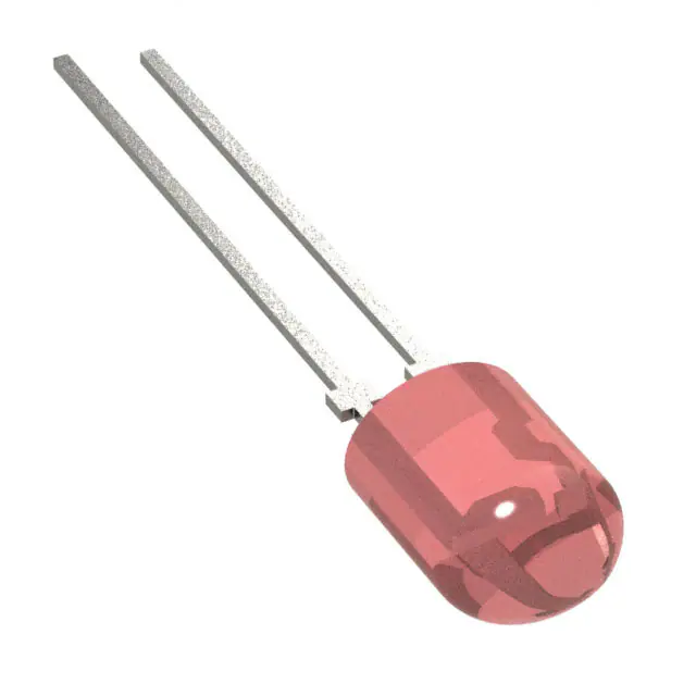
4 mm Standard Oval LEDs
Data Sheet
Description
Features
These Precision Optical Performance Oval LEDs are specifically designed for billboard sign application. The oval
shaped radiation pattern with optimal viewing angle
and enhance high luminous intensity ensure that these
devices are excellent for this outdoor applications. The
package epoxy contains UV inhibitor to reduce the
effects of long term exposure to direct sunlight.
x Well defined spatial radiation pattern
x High brightness material
x Available in red, green and blue color
– Red AlInGaP 626 nm
– Green InGaN 530 nm
– Blue InGaN 470 nm
x Superior resistance to moisture
Applications
x Standoff Package
x Billboard Sign
x Tinted and diffused
x Full Color Signs
x Typical viewing angle 40° x 100°
Package Dimensions
21.0
MIN.
0.827
7.26 ± 0.20
0.286 ± 0.008
1.25 ± 0.20
0.049 ± 0.008
1.0
MIN.
0.039
3.00 ± 0.20
0.118 ± 0.008
CATHODE LEAD
2.54 ± 0.30
0.100 ± 0.012
3.80 ± 0.20
0.1496 ± 0.008
10.00 ± 0.50
0.394 ± 0.020
0.80
MAX. EPOXY MENISCUS
0.031
Sq Typ.
0.50 ± 0.10
0.020 ± 0.004
NOTE:
1. MEASURED AT BASE OF LENS.
Notes:
All dimensions in millimeters (inches).
Tolerance is ± 0.20 mm unless other specified
Caution: InGaN devices are Class 1C HBM ESD sensitive per JEDEC Standard. Please observe appropriate
precautions during handling and processing. Refer to Application Note AN-1142 for additional details.
�Device Selection Guide
Part Number
Color and Dominant
Wavelength Od (nm) Typ
HLMP-LG75-XY0DD
HLMP-LM75-34CDD
HLMP-LB75-VWBDD
Luminous Intensity Iv (mcd)
at 20 mA [1,2,5]
Min
Max
Typical Viewing Angle (°)
Red 626
1660
2400
40x100
Green 530
4200
6050
40x100
Blue 470
1150
1660
40x100
Notes:
1. The luminous intensity is measured on the mechanical axis of the lamp package and it is tested with pulsing condition.
2. The optical axis is closely aligned with the package mechanical axis.
3. Dominant wavelength, Od, is derived from the CIE Chromaticity Diagram and represents the color of the lamp.
4. T½ is the off-axis angle where the luminous intensity is half the on-axis intensity.
5. Tolerance for each bin limit is ± 15%.
Part Numbering System
H L MP – L x 7 5 – x x x xx
Packaging Option
DD: Ammopack
Color Bin Selection
0 : Full Distribution
B : Color Bin 2 and 3
C : Color Bin 3 and 4
Maximum Intensity Bin
Refer to Device Selection Guide
Minimum Intensity Bin
Refer to Device Selection Guide
Color
G : Red
M : Green
B : Blue
Package
L: 4 mm Standard Oval
Note: Please refer to AB 5337 for complete information about part numbering system
2
�Absolute Maximum Ratings
TJ = 25°C
Parameter
Red
Green/ Blue
Unit
DC Forward Current [1]
50
30
mA
Peak Forward Current
100 [2]
100 [3]
mA
Power Dissipation
120
114
mW
LED Junction Temperature
130
110
°C
Operating Temperature Range
-40 to +100
Storage Temperature Range
-40 to +85
°C
-40 to +100
°C
Notes:
1. Derate linearly as shown in Figures 4 and 8.
2. Duty Factor 30%, frequency 1 KHz.
2. Duty Factor 10%, frequency 1 KHz.
Electrical / Optical Characteristics
TJ = 25°C
Parameter
Symbol
Forward Voltage
Red
Green
Blue
VF
Reverse Voltage [3]
Red
Green and Blue
VR
Dominant Wavelength [1]
Red
Green
Blue
Od
Peak Wavelength
Red
Green
Blue
OPEAK
Thermal Resistance
RTJ-PIN
Luminous Efficacy [2]
KV
Red
Green
Blue
Min.
Typ.
Max.
1.8
2.8
2.8
2.1
3.2
3.2
2.4
3.8
3.8
Units
Test Conditions
V
IF = 20 mA
V
IR = 100 PA
IR = 10 PA
5
5
618
527
464
626
530
470
nm
IF = 20 mA
nm
Peak of Wavelength of Spectral
Distribution at IF = 20 mA
°C/W
LED Junction-to-Pin
lm/W
Emitted Luminous Power/
Emitted Radiant Power
630
535
472
634
526
464
240
218
538
65
Notes:
1. The dominant wavelength is derived from the chromaticity Diagram and represents the color of the lamp.
2. The radiant intensity, Ie in watts per steradian, may be found from the equation Ie = IV/KV where IV is the luminous intensity in candelas and KV is
the luminous efficacy in lumens/watt.
3. Indicates product final testing condition. Long term reverse bias is not recommended.
3
�1
100
0.8
80
FORWARD CURRENT - mA
RELATIVE INTENSITY
AlInGaP Red
0.6
0.4
0.2
0
550
600
650
WAVELENGTH - nm
0
20
40
60
DC FORWARD CURRENT-mA
Figure 3. Relative Intensity vs Forward Current
4
20
0
1
2
FORWARD VOLTAGE - V
3
Figure 2. Forward Current vs Forward Voltage
IF MAX - MAXIMUM FORWARD CURRENT - mA
RELATIVE LUMINOUS INTENSITY
(NORMALIZED AT 20mA)
5.0
4.5
4.0
3.5
3.0
2.5
2.0
1.5
1.0
0.5
0.0
40
0
700
Figure 1. Relative Intensity vs Wavelength
60
80
100
60
50
40
30
20
10
0
0
20
40
60
80
TA - AMBIENT TEMPERATURE - °C
Figure 4. Maximum Forward Current vs Ambient Temperature
100
�1.0
0.9
0.8
0.7
0.6
0.5
0.4
0.3
0.2
0.1
0.0
100
BLUE
FORWARD CURRENT - mA
RELATIVE INTENSITY
InGaN Green and Blue
GREEN
380
430
480
530
WAVELENGTH - nm
580
630
0
0
35
3.0
30
Green
2.5
2.0
Blue
1.5
1.0
0
20
40
60
80
FORWARD CURRENT-mA
100
120
Figure 7. Relative Intensity vs Forward Current
RELATIVE DOMINANT WAVELENGTH-nm
20
3.5
0.0
4
2
0
Blue
-2
-4
Green
-6
0
20
1
2
3
FORWARD VOLTAGE - V
4
5
40
60
80
TA - AMBIENTTEMPERATURE - °C
100
40
60
80
FORWARD CURRENT-mA
25
20
15
10
5
0
0
20
Figure 8. Maximum Forward Current vs Ambient Temperature
6
Figure 9. Relative Dominant Wavelength vs Forward Current
5
40
Figure 6. Forward Current vs Forward Voltage
0.5
-8
60
IFmax - MAXIMUM FORWARD
CURRENT - mA
RELATIVE INTENSITY
(NORMALIZED AT 20mA)
Figure 5. Relative Intensity vs Wavelength
80
100
120
�1.0
0.8
0.8
NORMALIZED INTENSITY
NORMALIZED INTENSITY
1.0
0.6
0.4
LG75 Red
LM75
LB75
0.2
0.0
-90
-60
-30
0
30
ANGULAR DISPALCEMENT (°)
60
Figure 10. Radiation pattern-Major Axis
0.4
0.2
-90
-60
-30
0
30
ANGULAR DISPALCEMENT (°)
60
90
Figure11. Radiation pattern-Minor Axis
0.5
10
Green
Red
Blue
Green
Red
Blue
0.4
FORWARD VOLTAGE SHIFT-V
RELATIVE LIGHT OUTPUT
(NORMALIZED AT TJ = 25°C)
0.6
0.0
90
LG75 Red
LM75
LB75
1
0.3
0.2
0.1
0
-0.1
-0.2
-0.3
0.1
-40
-20
0
20
40
60
80 100
TJ -JUNCTION TEMPERATURE
120
-0.4
140
-40
-20
0
20 40
60 80 100
TJ -JUNCTION TEMPERATURE
Figure12. Relative Light Output vs Junction Temperature
Figure13. Forward Voltage Shift vs Junction Temperature
Intensity Bin Limit Table (1.2: 1 Iv Bin Ratio)
VF Bin Table (V at 20 mA)
Bin
Intensity (mcd) at 20 mA
Bin ID
Min
Max
Min
Max
VD
1.8
2.0
V
1150
1380
VA
2.0
2.2
W
1380
1660
VB
2.2
2.4
X
1660
1990
Y
1990
2400
Z
2400
2900
1
2900
3500
2
3500
4200
3
4200
5040
4
5040
6050
Tolerance for each bin limit is ±15%
6
Notes:
1. Tolerance for each bin limit is ±0.05 V
2. VF binning only applicable to Red color.
120
140
�Red Color Range
Blue Color Bin Table
Min
Dom
Max
Dom
Min
Bin Dom
Max
Dom
618.0
630.0
2
468.0
x
0.6872
0.3126
0.6890
0.2943
y
0.6690
0.3149
0.7080
0.2920
Tolerance for each bin limit is r 0.5 nm
3
Green Color Bin Table
Min
Bin Dom
Max
Dom
3
531
527
4
531
535
464.0
468.0
472.0
x
0.1305
0.1711
0.1967
0.1625
y
0.8189
0.7218
0.7077
0.8012
x
0.1625
0.1967
0.221
0.1929
y
0.8012
0.7077
0.692
0.7816
1.000
0.800
3 4
Green
Y
0.600
0.400
Red
0.200
Blue
7
0.100
0.1766
0.1699
0.1291
0.0966
0.1062
0.0495
x
0.1291
0.1699
0.1616
0.1187
y
0.0495
0.1062
0.1209
0.0671
Note:
1. All bin categories are established for classification of products.
Products may not be available in all bin categories. Please contact
your Avago representative for further information.
Avago Color Bin on CIE 1931 Chromaticity Diagram
0.000
0.000
0.1374
0.0374
Tolerance for each bin limit is r 0.5 nm
Tolerance for each bin limit is r 0.5 nm
3
x
y
2
0.200
0.300
0.400
X
0.500
0.600
0.700
0.800
�Precautions:
Lead Forming:
x The leads of an LED lamp may be preformed or cut to
length prior to insertion and soldering on PC board.
x For better control, it is recommended to use proper
tool to precisely form and cut the leads to applicable
length rather than doing it manually.
x If manual lead cutting is necessary, cut the leads after
the soldering process. The solder connection forms a
mechanical ground which prevents mechanical stress
due to lead cutting from traveling into LED package.
This is highly recommended for hand solder operation,
as the excess lead length also acts as small heat sink.
Note:
1. PCB with different size and design (component density) will have
different heat mass (heat capacity). This might cause a change in
temperature experienced by the board if same wave soldering
setting is used. So, it is recommended to re-calibrate the soldering
profile again before loading a new type of PCB.
2. Avago Technologies’ AllnGaP high brightness LED are using high
efficiency LED die with single wire bond as shown below. Customer
is advised to take extra precaution during wave soldering to ensure
that the maximum wave temperature does not exceed 260° C and
the solder contact time does not exceeding 5 sec. Over-stressing the
LED during soldering process might cause premature failure to the
LED due to delamination.
Avago Technologies LED configuration
Soldering and Handling:
x Care must be taken during PCB assembly and
soldering process to prevent damage to the LED
component.
x LED component may be effectively hand soldered
to PCB. However, it is only recommended under
unavoidable circumstances such as rework. The closest
manual soldering distance of the soldering heat
source (soldering iron’s tip) to the body is 1.59 mm.
Soldering the LED using soldering iron tip closer than
1.59 mm might damage the LED.
1.59mm
x ESD precaution must be properly applied on the
soldering station and personnel to prevent ESD
damage to the LED component that is ESD sensitive.
Do refer to Avago application note AN 1142 for details.
The soldering iron used should have grounded tip to
ensure electrostatic charge is properly grounded.
x Recommended soldering condition:
Wave
Soldering [1, 2]
Manual Solder
Dipping
Pre-heat temperature
105° C Max.
–
Preheat time
60 sec Max
–
Peak temperature
260° C Max.
260° C Max.
Dwell time
5 sec Max.
5 sec Max
Note:
1. Above conditions refers to measurement with thermocouple
mounted at the bottom of PCB.
2. It is recommended to use only bottom preheaters in order to
reduce thermal stress experienced by LED.
x Wave soldering parameters must be set and maintained according to the recommended temperature
and dwell time. Customer is advised to perform
daily check on the soldering profile to ensure that
it is always conforming to recommended soldering
conditions.
8
&$7+2'(
$12'(
$O,Q*D3�'HYLFH
,Q*D1�'HYLFH
x Any alignment fixture that is being applied during
wave soldering should be loosely fitted and should
not apply weight or force on LED. Non metal material
is recommended as it will absorb less heat during
wave soldering process.
x At elevated temperature, LED is more susceptible to
mechanical stress. Therefore, PCB must allowed to cool
down to room temperature prior to handling, which
includes removal of alignment fixture or pallet.
x If PCB board contains both through hole (TH) LED and
other surface mount components, it is recommended
that surface mount components be soldered on the
top side of the PCB. If surface mount need to be on the
bottom side, these components should be soldered
using reflow soldering prior to insertion the TH LED.
x Recommended PC board plated through holes (PTH)
size for LED component leads.
LED component
lead size
Diagonal
Plated through
hole diameter
0.45 x 0.45 mm
(0.018x 0.018 inch)
0.636 mm
(0.025 inch)
0.98 to 1.08 mm
(0.039 to 0.043 inch)
0.50 x 0.50 mm
(0.020x 0.020 inch)
0.707 mm
(0.028 inch)
1.05 to 1.15 mm
(0.041 to 0.045 inch)
x Over-sizing the PTH can lead to twisted LED after
clinching. On the other hand under sizing the PTH can
cause difficulty inserting the TH LED.
Refer to application note AN5334 for more information about
soldering and handling of high brightness TH LED lamps.
�Example of Wave Soldering Temperature Profile for TH LED
260° C Max
TEMPERATURE (° C)
Recommended solder:
Sn63 (Leaded solder alloy)
SAC305 (Lead free solder alloy)
Flux: Rosin flux
Solder bath temperature: 255° C ± 5° C
(maximum peak temperature = 260° C)
105° C Max
Dwell time: 3.0 sec - 5.0 sec
(maximum = 5 sec)
60 sec Max
Note: Allow for board to be sufficiently
cooled to room temperature before
exerting mechanical force.
TIME (sec)
Ammo Packs Drawing
6.35±1.30
0.25±0.0512
12.70±1.00
0.50±0.0394
CATHODE
20.5±1.00
0.8071±0.0394
9.125±0.625
0.3593±0.025
18.00±0.50
0.7087±0.0197
12.70±0.30
0.50±0.0118
Ø
0.70±0.20
0.276±0.0079
9
VIEW A - A
4.00±0.20
TYP.
0.1575±0.0079
�Packaging Box for Ammo Packs
FROM LEFT SIDE OF BOX
ADHESIVE TAPE MUST BE
FACING UPWARDS.
LABEL ON THIS
SIDE OF BOX
ANODE LEAD LEAVES
THE BOX FIRST.
Note: For InGaN device, the ammo pack packaging box contain ESD logo
Packaging Label
(i) Avago Mother Label: (Available on packaging box of ammo pack and shipping box)
�
��3��,WHP��3DUW�1XPEHU�
67$1'$5'�/$%(/�/6�����
5R+6�&RPSOLDQW�
H��������PD[�WHPS����&�
��7��/RW��/RW�1XPEHU�
�
�4��47
很抱歉,暂时无法提供与“HLMP-LG75-XY0DD”相匹配的价格&库存,您可以联系我们找货
免费人工找货- 国内价格 香港价格
- 1+8.483441+1.09781
- 10+5.9469610+0.76957
- 100+4.37912100+0.56669
- 500+3.67931500+0.47613
- 1000+3.450031000+0.44646
- 国内价格
- 1+5.23733
- 5+4.49030
- 25+4.12490
- 100+3.74327
- 200+3.36975
- 500+2.99624
- 1000+2.62272
- 2000+2.42785
- 国内价格 香港价格
- 2000+3.255552000+0.42129
- 4000+3.090584000+0.39994
- 6000+3.006046000+0.38900
- 10000+2.9106110000+0.37665