HLMP-Yxxx
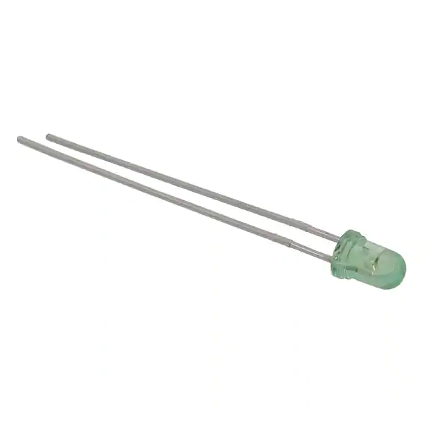
T-1 (3 mm) AlInGaP LED Lamps
Data Sheet
Description
Features
This family of T-1 lamps is widely used in general purpose
indicator and back lighting applications. The optical
design is balanced to yield superior light output and wide
viewing angles. Several intensity choices are available in
each color for increased design flexibility.
• High luminous intensity output
Applications
• Status indicator
• Backlighting front panels
• Light pipe sources
• Low power consumption
• Choice of bright colors
– Deep Red
– Red
– Red-Orange
– Orange
– Amber
– Green
• High efficiency
• Lighted switches
• Versatile mounting on PCB or panel
• I.C. Compatible/low current requirement
• Popular T-1 diameter package
• Reliable and rugged
• RoHS compliant
Package Dimension
5.2
0.205
4.1 ± 0.2
0.161 ± 0.008
24.0 (MIN)
0.945
1.0 (MAX)
0.04
CATHODE
3.8 3.5
3.1 ± 0.2
0.15 0.138 0.122 ± 0.008
1.0 (MIN)
0.04
2.54
0.1
0.45 x 0.4 TYP
(0.018 x 0.016)
Notes:
1. All dimensions are in millimeter (inches).
2. Tolerance is ±0.25mm (.010) unless otherwise stated.
3. Lead spacing is measured where the leads emerge from the package.
�Selection Guide
Luminous Intensity, Iv (mcd) @ 20 mA
Color
Part Number
Package Description
Min.
Typ.
Deep Red
HLMP-Y651-G00xx
Untinted, Non-diffused
140
300
Red
HLMP-Y601-J00xx
Untinted, Non-diffused
240
680
Red-Orange
HLMP-Y951-K00xx
Untinted, Non-diffused
310
680
Yellow Orange
HLMP-Y901-J00xx
Untinted, Non-diffused
240
680
HLMP-Y902-J00xx
Tinted, Non-diffused
240
680
Amber
HLMP-Y701-G00xx
Untinted, Non-diffused
140
400
Green
HLMP-Y802-F00xx
Tinted, Non-diffused
110
240
Part Numbering System
HLMP - Y x x x - x x x xx
Mechanical Options
00: Bulk
Color Bin Options
0: Full Color Bin Distribution
Maximum IV Bin Options
0: Open (no max. limit)
Others: Please refer to the IV Bin Table
Minimum IV Bin Options
Please refer to the IV Bin Table
2
Max.
Viewing Angle,
2θ½ (°)
45
�Absolute Maximum Ratings at TA = 25°C
Parameter
HLMP-Yxxx
Units
DC Forward Current
20
mA
Peak Forward Current
(1/10 Duty Cycle, 0.1ms Pulse Width)
60
mA
Reverse Voltage (IR = 100µA)
5
V
Junction Temperature
110
°C
Power Dissipation
48
mW
Storage Temperature Range
-40 to +100
°C
Operating Temperature Range
-40 to +100
°C
Electrical /Optical Characteristic at TA = 25°C
Description
Symbol
Part Number
Min.
Typ.
Peak Wavelength
λPEAK
HLMP-Y651
HLMP-Y601
HLMP-Y951
HLMP-Y90x
HLMP-Y701
HLMP-Y802-F00xx
Dominant Wavelength
λd
HLMP-Y651
HLMP-Y601
HLMP-Y951
HLMP-Y90x
HLMP-Y701
HLMP-Y802-F00xx
Spectrum Half Width
∆λ
HLMP-Y651
HLMP-Y601
HLMP-Y951
HLMP-Y90x
HLMP-Y701
HLMP-Y802-F00xx
15
15
17
17
15
11
Forward Voltage
VF
HLMP-Y651
HLMP-Y601
HLMP-Y951
HLMP-Y90x
HLMP-Y701
HLMP-Y802-F00xx
2.0
2.0
2.0
2.0
2.0
2.1
Max.
652
633
622
611
595
575
635.0
620.0
610.0
599.5
582.0
564.5
638.0
627.0
615.0
605.0
592.0
572.0
646.0
635.0
620.0
610.5
597.0
576.5
Units
Test Conditions
nm
Measurement at peak
nm
Note 1
nm
2.2
2.2
2.2
2.4
2.2
2.4
V
Notes:
1. The dominant wavelength, λd, is derived from the Chromaticity Diagram and represents the color of the lamp.
3
IF = 20mA
(Figure 1)
�1
RELATIVE LUMINOUS INTENSITY
(NORMALIZED AT 20mA)
FORWARD CURRENT-mA
20
18
16
14
12
10
8
6
4
2
0
GREEN
DEEP RED, RED
RED-ORANGE, AMBER
YELLOW-ORANGE
0
0.5
1
1.5
FORWARD VOLTAGE-V
2
0.4
0.2
0
0
5
10
15
DC FORWARD CURRENT - mA
1
NORMALIZED INTENSITY
20
15
10
5
0
10
20
30
40
50
60
70
80
90 100 110
AMBIENT TEMPERATURE - °C
Figure 3. Ambient Temperature vs. Maximum DC Forward Current.
0.75
0.5
0.25
0
-90
-60
-30
0
30
60
ANGULAR DISPLACEMENT - DEGREES
Figure 4. Relative Luminous Intensity vs. Angular Displacement for
HLMP-Y651, HLMP-Y601, HLMP-Y951 and HLMP-Y701.
NORMALIZED INTENSITY
1
0.75
0.5
0.25
0
-90
-60
-30
0
30
60
ANGULAR DISPLACEMENT - DEGREES
Figure 5. Relative Luminous Intensity vs. Angular Displacement for
HLMP-Y90x and HLMP-Y80x.
4
20
Figure 2. Relative Luminous Intensity vs. Forward Current.
25
FORWARD CURRENT - mA
0.6
2.5
Figure 1. Forward Current vs. Forward Voltage.
0
0.8
90
Figure 6. Wavelength vs. Relative Luminous Intensity.
90
�Precautions:
Intensity Bin Limits
Intensity Range (mcd)
Assembly method:
Bin
Min.
Max.
F
110.0
140.0
G
140.0
180.0
H
180.0
240.0
J
240.0
310.0
K
310.0
400.0
L
400.0
520.0
M
520.0
680.0
N
680.0
880.0
P
880.0
1150.0
Q
1150
1500
This product is not meant for auto-insertion.
Lead Forming:
• The leads of an LED lamp may be preformed or cut to
length prior to insertion and soldering into PC board.
Tolerance for each bin limit is 15%.
Color Bin Limits Table
Lambda (nm)
Color
Category #
Min.
Max.
Red-Orange
1
610.5
613.5
2
613.5
616.5
3
616.5
619.5
2
599.5
602.0
3
602.0
604.5
4
604.5
607.5
5
607.5
610.5
1
584.5
587.0
2
587.0
589.5
4
589.5
592.0
6
592.0
594.5
7
594.5
597.0
2
573.5
576.5
3
570.5
573.5
4
567.5
570.5
5
564.5
567.5
YellowOrange
Amber
Green
Tolerance for each bin limit is ±1.0 nm.
5
• If lead forming is required before soldering, care must
be taken to avoid any excessive mechanical stress
induced to LED package. Otherwise, cut the leads
of LED to length after soldering process at room
temperature. The solder joint formed will absorb the
mechanical stress of the lead cutting from traveling to
the LED chip die attach and wirebond.
• During lead forming, the leads should be bent at a
point at least 3mm from the base of the lens. Do not
use the base of the lead frame as a fulcrum during
forming. Lead forming must be done before soldering
at normal temperature.
• It is recommended that tooling made to precisely form
and cut the leads to length rather than rely upon hand
operation.
�Precautions: (cont.)
Soldering Conditions:
• Care must be taken during PCB assembly and soldering
process to prevent damage to LED component.
• The closest LED is allowed to solder on board is 1.59
mm below the body (encapsulant epoxy) for those
parts without standoff.
• Recommended soldering conditions:
Wave Soldering
Manual Solder
Dipping
Pre-heat Temperature
105°C Max.
–
Pre-heat Time
60 sec Max.
–
Peak Temperature
250°C Max.
260°C Max.
Dwell Time
3 sec Max.
5 sec Max.
• Wave soldering parameter must be set and maintained
according to recommended temperature and dwell
time in the solder wave. Customer is advised to
periodically check on the soldering profile to ensure
the soldering profile used is always conforming to
recommended soldering condition.
• If necessary, use fixture to hold the LED component
in proper orientation with respect to the PCB during
soldering process.
• Proper handling is imperative to avoid excessive
thermal stresses to LED components when heated.
• Therefore, the soldered PCB must be allowed to cool to
room temperature, 25°C, before handling.
• Special attention must be given to board fabrication,
solder masking, surface plating and lead holes size and
component orientation to assure solderability.
• Recommended PC board plated through hole sizes for
LED component leads:
Diagonal
Plated Through
Hole Diameter
0.457 x 0.457 mm
(0.018 x 0.018 inch)
0.646 mm
(0.025 inch)
0.976 to 1.078 mm
(0.038 to 0.042 inch)
0.508 x 0.508 mm
(0.020 x 0.020 inch)
0.718 mm
(0.028 inch)
1.049 to 1.150 mm
(0.041 to 0.045 inch)
Note: Refer to application note AN1027 for more information on
soldering LED components.
Recommended solder:
Sn63 (Leaded solder alloy)
SAC305 (Lead free solder alloy)
LAMINAR WAVE
HOT AIR KNIFE
TURBULENT WAVE
250
LED Component
Lead Size
Flux: Rosin flux
TEMPERATURE (°C)
200
Solder bath temperature:
245°C± 5°C (maximum peak
temperature = 250°C)
150
Dwell time: 1.5 sec - 3.0 sec
(maximum = 3sec)
100
Note: Allow for board to be
sufficiently cooled to room
temperature before exerting
mechanical force.
50
PREHEAT
0
10
20
30
40
60
50
TIME (SECONDS)
70
80
90
100
Figure 7. Recommended wave soldering profile.
Avago’s products and software are not specifically designed, manufactured or authorized for sale as
parts, components or assemblies for the planning, construction, maintenenace or direct operation of a
nuclear facility or for use in medical devices or applications. Customer is solely responsible, and waives all rights
to make claims against avago or its suppliers, fo all loss, damage, expense or liability in connection with such use.
For product information and a complete list of distributors, please go to our web site:
www.avagotech.com
Avago, Avago Technologies, and the A logo are trademarks of Avago Technologies in the United States and other countries.
Data subject to change. Copyright © 2005-2014 Avago Technologies. All rights reserved.
AV02-1664EN - July 26, 2014
�
很抱歉,暂时无法提供与“HLMP-Y802-F0000”相匹配的价格&库存,您可以联系我们找货
免费人工找货