HSCH-53xx Series
Beam Lead Schottky Diodes for Mixers and Detectors
(1-26 GHz)
Data Sheet
Description
These beam lead diodes are constructed using a metalsemiconductor Schottky barrier junction. Advanced
epitaxial techniques and precise process control insure
uniformity and repeatability of this planar passivated
microwave semiconductor. A nitride passivation layer
provides immunity from contaminants which could
otherwise lead to IR drift.
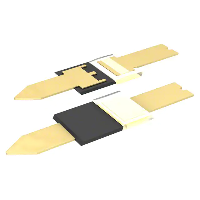
The Avago beam lead process allows for large beam
anchor pads for rugged construction (typical 6 gram
pull strength) without degrading capacitance.
Applications
The beam lead diode is ideally suited for use in stripline
or microstrip circuits. Its small physical size and
uniform dimensions give it low parasitics and repeatable
RF characteristics through K-band.
The basic medium barrier devices in this family are DC
tested HSCH-5310 and -5312. Equivalent low barrier
devices are HSCH-5330 and -5332. Batch matched
versions are available as HSCH-5331.
The HSCH-5340 is selected for applications requiring
guaranteed RF-tested performance up to 26 GHz. The
HSCH-5314 is rated at 7.2 dB maximum noise figure at
16 GHz.
Assembly Techniques
Thermocompression bonding is recommended. Welding
or conductive epoxy may also be used. For additional
information, see Application Note 979, The Handling
and Bonding of Beam Lead Devices Made Easy, or
Application Note 993, Beam Lead Device Bonding to
Soft Substances.
Features
• Platinum tri-metal system
High temperature stability
• Silicon nitride passivation
Stable, reliable performance
• Low noise figure
Guaranteed 7.5 dB at 26 GHz
• High uniformity
Tightly controlled process insures uniform RF
characteristics
• Rugged construction
4 grams minimum lead pull
• Low capacitance
0.10 pF max. at 0 V
• Polyimide scratch protection
Outline 07
CATHODE
GOLD LEADS
130 (5)
100 (4)
135 (5)
90 (3)
135 (5)
90 (3)
225 (9)
200 (8)
310 (12)
250 (10)
225 (9)
170 (7)
8 Min. (.3)
30 MIN (1)
SILICON
GLASS
710 (28)
670 (26)
DIMENSIONS IN µm (1/1000 inch)
60 (2)
40 (1)
�Maximum Ratings
Pulse Power Incident at TA = 25°C ........................................................ 1 W
Pulse Width = 1 ms, Du = 0.001
CW Power Dissipation at TA = 25°C ............................................... 150 mW
Measured in an infinite heat sink derated linearly
to zero at maximum rated temperature
TOPR – Operating Temperature Range ............................. -65°C to +175 °C
TSTG – Storage Temperature Range ................................... -65°C to +200°C
Minimum Lead Strength ...................................... 4 grams pull on any lead
Diode Mounting Temperature .............................. +350°C for 10 sec. max.
These diodes are ESD sensitive. Handle with care to avoid static
discharge through the diode.
Table IA. Electrical Specifications for RF Tested Diodes at TA = 25°C
Part
Number
HSCH-
Barrier
5314
Medium
5340
Low
Min.
Max.
Max.
SWR
Min.
Breakdown
Voltage
VBR (V)
7.2 at
16 GHz
200
400
1.5:1
4
7.5 at
26 GHz
150
350
Max.
Noise
Figure
NF (dB)
Test
Conditions
*Minimum batch size 20 units.
Note:
1. CT = CJ + 0.02 pF (fringing cap).
2
IF
Impedance
Ω)
ZIF (Ω
DC Load Resistance - 0 Ω
LO Power = 1 mW
IF = 30 MHz, 1.5 dB NF
IR ≤ 10 µA
Max.
Dynamic
Resistance
Ω)
RD (Ω
Max.
Total
Capacitance
CT (pF)
Max.
Forward
Voltage
VF (mV)
Max.
Leakage
Current
IR (nA)
16
0.15
500
100
20
0.10
375
400
IF = 5 mA
VR = 0 V
f = 1 MHz
IF = 1 mA
VR = 1 V
�Table IB. Electrical Specifications for DC Tested Diodes at TA = 25°C
Part
Number
HSCH-
Batch*
Matched
HSCH-
5312
5310
5332
5330
5331
Test
Conditions
∆VF ≤ 15 mV
@ 5 mA
Barrier
Minimum
Breakdown
Voltage
VBR (V)
Maximum
Dynamic
Resistance
Ω)
RD (Ω
Maximum
Total
Capacitance
CT (pF)
Maximum
Forward
Voltage
VF (mV)
Maximum
Leakage
Current
IR (nA)
Medium
4
16
20
0.15
0.10
500
100
Low
4
16
20
0.15
0.10
375
400
IR ≤ 10 µA
IF = 5 mA
VR = 0 V
f = 1 MHz
IF = 1 mA
VR = 1 V
*Minimum batch size 20 units.
Typical Detector Characteristics at TA = 25°C
Medium Barrier and Low Barrier (DC Bias)
Parameter
Symbol
Typical Value
Units
Test Conditions
TSS
–54
dBm
Voltage Sensitivity
γ
6.6
mV/µW
20 µA Bias, RL = 100 kΩ
Video Bandwidth = 2 MHz
f = 10 GHz
Video Resistance
RV
1400
Ω
Symbol
Typical Value
Units
Test Conditions
TSS
–44
dBm
Voltage Sensitivity
γ
10
mV/µW
Zero Bias, RL = 10 MΩ
Video Bandwidth = 2 MHz
f = 10 GHz
Video Resistance
RV
1.8
MΩ
Tangential Sensitivity
Low Barrier (Zero Bias)
Parameter
Tangential Sensitivity
SPICE Parameters
Parameter
BV
CJO
EG
IBV
IS
N
RS
PB
PT
M
3
Units
V
pF
eV
A
A
Ω
V
HSCH-5312
HSCH-5314
5
0.13
0.69
10E-5
3 x 10E-10
1.08
9
0.65
2
0.5
HSCH-5310
5
0.09
0.69
10E-5
3 x 10E-10
1.08
13
0.65
2
0.5
HSCH-5330
HSCH-5340
5
0.09
0.69
10E-5
4 x 10E-8
1.08
13
0.5
2
0.5
HSCH-5332
5
0.13
0.69
10E-5
4 x 10E-8
1.08
9
0.5
2
0.5
�Typical Parameters
100
10
1
0.1
1
0.4
0.6
0.8
6.5
0.15 pF
6.0
0.25 pF
5.5
1.0
0
0.2
0.4
0.6
5.0
0.8
0
4
2
Figure 1. Typical forward characteristics for
medium barrier beam lead diodes. HSCH-5310
series.
16
0.5
2.0
26 GHz
5.0
2.0
0.2
20
10.0
3.0
5.0
150 µA
26 GHz
10
2
10.0
10.0
0.2
5.0
3.0
1.0
0.5
0.2
5.0
10.0
3.0
2.0
1.0
2
0.5
28
26
20 µA
50 µA
3.0
0.2
24
Figure 3. Typical noise figure vs. frequency.
Figure 2. Typical forward characteristics for
low barrier beam lead diodes. HSCH-5330,
-5340 series.
18
10.0
0.2
5.0
5.0
3.0
3.0
0.5
0.5
2.0
2.0
1.0
Figure 4. Typical admittance characteristics with 1 mA self bias.
HSCH-5340.
4
20
1.0
0.5
10
12
9.375
FREQUENCY (GHz)
1.0
0.2
8
FORWARD VOLTAGE (V)
FORWARD VOLTAGE (V)
10.0
0.2
0.1 pF
0.1
0.01
0
7.0
10
2.0
0.01
7.5
+125°C
+25°C
–55°C
NOISE FIGURE (dB)
+125°C
+25°C
–55°C
FORWARD CURRENT (mA)
FORWARD CURRENT (mA)
100
1.0
Figure 5. Typical admittance characteristics with external bias.
HSCH-5340.
�1.0
0.2
1 mA
1.5 mA
3 mA
18 GHz
1.0
20 µA
50 µA
0.5
2.0
2.0
150 µA
18 GHz
3.0
3.0
10
5.0
10
0.2
5.0
10.0
10.0
5.0
3.0
2.0
1.0
0.2
5.0
10.0
0.2
0.5
2
10.0
3.0
2.0
1.0
0.5
0.2
2
10.0
0.2
5.0
5.0
3.0
0.5
10.0
0.5
3.0
0.5
2.0
2.0
1.0
1.0
Figure 6. Typical admittance characteristics with self bias.
HSCH-5314.
Figure 7. Typical admittance characteristics with external bias.
HSCH-5314.
Models for Each Beam Lead Schottky Diode
HSCH-5340
1 mA Self Bias
0.03 pF
0.1 nH
0.04 nH
11 Ω
267 Ω
0.11 pF
Other HSCH-53xx
Self Bias
0.02 pF
0.1 nH
Rs
Rj
Cj
Part Numbers
HSCH-5314
5
1.0 mA Self Bias
RS (Ω)
Rj (Ω)
Cj (pF)
5.0
393
0.11
1.5 mA Self Bias
RS (Ω)
Rj (Ω)
Cj (pF)
5.2
232
0.11
3.0 mA Self Bias
RS (Ω)
Rj (Ω)
Cj (pF)
5.0
150
0.12
�HSCH-5340
External Bias
0.03 pF
0.1 nH
Rj
0.04 nH
11 Ω
Cj
0.11 pF
20 µA DC Bias
Rj (Ω)
Cj (pF)
1300
0.09
Part Numbers
HSCH-5340
50 µA DC Bias
Rj (Ω)
Cj (pF)
560
0.09
150 µA DC Bias
Rj (Ω)
Cj (pF)
187
0.10
Other HSCH-53xx
External Bias
0.02 pF
0.1 nH
Rs
Rj
Cj
Part Numbers
HSCH-5314
20 µADC Bias
RS (Ω)
Rj (Ω) Cj (pF)
2.8
1300
0.11
For product information and a complete list of distributors, please go to our website:
50 µADC Bias
RS (Ω)
Rj (Ω)
Cj (pF)
4.7
520
0.12
www.avagotech.com
Avago, Avago Technologies, and the A logo are trademarks of Avago Technologies Limited in the United States and other countries.
Data subject to change. Copyright © 2006 Avago Technologies Pte. All rights reserved. Obsoletes AV01-0127EN
AV01-0484EN September 21, 2006
150 µADC Bias
RS (Ω)
Rj (Ω)
Cj (pF)
2.7
180
0.13
�
很抱歉,暂时无法提供与“HSCH-5330”相匹配的价格&库存,您可以联系我们找货
免费人工找货