HSMW-C280
Miniature ChipLED
Data Sheet
Feature
LED with InGaN die
Surface mount device with 0402 footprint
Compatible with reflow soldering
Tape in 8mm carrier tape on a 7 inch diameter reel
Application
Backlighting
Indicator
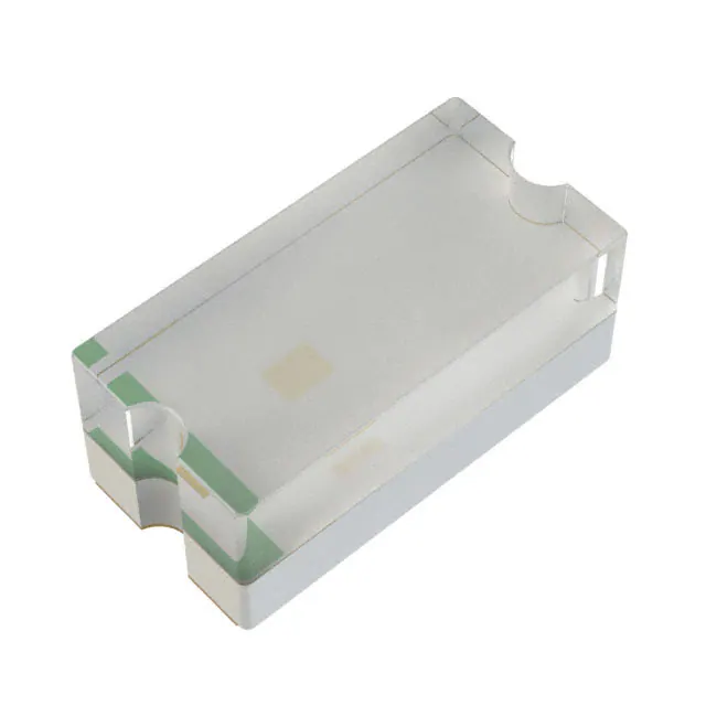
Package Dimension
Note:
1.
2.
All dimensions are in millimeters (inches).
Tolerance ±0.1mm (±0.004in) unless otherwise specified.
Caution: LEDs are ESD sensitive. Please observe appropriate precautions during handling and processing. Refer
to Application Note AN-1142 for additional details.
1
�Absolute Maximum Value at TA = 25°C
Parameter
White
Unit
Forward Current1
20
mA
Peak Pulsing Current2
100
mA
Power Dissipation
78
mW
LED Junction Temperature
95
°C
Operating Temperature Range
-30 to 85
°C
Storage Temperature Range
-40 to 85
°C
Note:
1.
2.
Derate as shown in Figure 8.
Pulse condition of 1/10 duty and 0.1ms width.
Optical Characteristics at TA = 25°C, IF=20mA
Color
Luminous Intensity
Viewing
Iv (mcd)1
Angle
2θ1/22
White
Min
Typ
Typ
180.0
262.7
130
Note:
1.
2.
The luminous intensity is measured at the mechanical axis of the LED package. The actual peak of the
spatial radiation pattern may not be aligned with the axis.
Viewing angle is the off axis angle where the luminous intensity is ½ the peak intensity.
Electrical Characteristics at TA = 25°C, IF=20mA
Color
Forward Voltage Vf (V)1
Reverse Voltage
Vr(V) @Ir=100μA
Thermal
2
Resistance
Rθj-pin(°C/W)
White
Min
Max
Min
Typ
2.7
3.9
5
300
Note:
1.
2.
Forward voltage tolerance is ±0.1V.
Reverse voltage Indicates product final testing, long terms reverse bias is not recommended.
2
�Luminous Intensity Bin Limits
Bin ID
Luminous Intensity (mcd)
Min
180.0
285.0
450.0
S
T
U
Tolerance ±15%
White Color Bin Limits
Bin ID
Chromaticity Coordinates
x
y
A1
0.270
0.246
0.270
0.278
0.250
0.250
0.250
0.218
A2
0.270
0.246
0.270
0.213
0.250
0.185
0.250
0.218
B1
0.270
0.246
0.270
0.278
0.290
0.306
0.290
0.274
B2
0.270
0.246
0.270
0.213
0.290
0.241
0.290
0.274
Tolerance ±0.02
Max
285.0
450.0
715.0
Bin ID
C1
C2
D1
D2
0.38
0.36
0.34
D1
0.32
C1
0.30
0.28
C2
B1
y
D2
0.26
A1
0.24
0.22
B2
A2
0.20
0.18
0.16
0.24 0.26 0.28 0.30 0.32 0.34
x
Figure 1. Chromaticity diagram
3
Chromaticity Coordinates
x
y
0.290
0.306
0.310
0.336
0.310
0.303
0.290
0.274
0.290
0.241
0.310
0.271
0.310
0.303
0.290
0.274
0.310
0.303
0.310
0.336
0.330
0.365
0.330
0.333
0.310
0.303
0.310
0.271
0.330
0.300
0.330
0.333
�Forward Voltage Bin Limits
Bin ID
Forward Voltage (V)
Min
2.7
2.9
3.1
3.3
3.5
3.7
Z
1
2
3
4
5
Tolerance ±0.1V
Max
2.9
3.1
3.3
3.5
3.7
3.9
20
18
FORWARD CURRENT - mA
RELATIVE LUMINOUS INTENSITY
(NORMALIZED AT 20 mA)
1.0
0.8
0.6
0.4
16
14
12
10
0.2
8
6
4
2
0.0
0
0
2
4
6
8 10 12 14 16 18 20
1
FORWARD CURRENT - mA
2
2.5
430
3.5
Figure 3. Forward Current vs Forward Voltage
1.0
0.9
0.8
0.7
0.6
0.5
0.4
0.3
0.2
0.1
0.0
380
3
FORWARD VOLTAGE - V
Figure 2. Luminous Intensity vs Forward Current
RELATIVE INTENSITY
1.5
480
530
580
630
WAVELENGTH - nm
Figure 4. Spectrum
4
680
730
780
4
�0.014
x
0.012
0.8
COORDINATE SHIFT
NORMALIZED INTENSITY
1.0
0.5
0.3
y
0.010
0.008
0.006
0.004
0.002
0.0
0.000
-90
-60
-30
0
30
60
90
0
2
ANGULAR DISPLACEMENT - DEGREES
Figure 5. Radiation pattern
4
6
8 10 12 14 16
FORWARD CURRENT - mA
18
Figure 6. Chromaticity shift vs Forward current
1.2
22
20
Rj-a=500°C/W
Rj-a=600°C/W
Rj-a=700°C/W
Rj-a=850°C/W
18
FORWARD CURRENT - mA
RELATIVE INTENSITY
1.0
0.8
0.6
0.4
0.2
16
14
12
10
8
6
4
2
0.0
0
-40
-20
0
20
40
60
80
100
0
AMBIENT TEMPERATURE, TA -°C
Figure 7. Relative intensity vs Temperature
10
20
30
40
50
60
70
80
AMBIENT TEMPERATURE - °C
Figure 8. Derating curve
Figure 9. Recommended solder pad
5
90
100
20
�Figure 10. Reel orientation
Figure 11. Reel dimensions
6
�Figure 12. Carrier tape dimensions
Soldering
Recommended reflow soldering condition:
(a) Reflow soldering must not be done more than 2 times. Do observe necessary precautions of handling moisture sensitive
device as stated in below section.
(b) Do not apply any pressure or force on the LED during reflow and after reflow when the LED is still hot.
(c) It is preferred to use reflow soldering to solder the LED. But if unavoidable (such as rework), manual hand soldering can be
used but must be strictly controlled to condition below:
Soldering iron tip temperature = 310°C max
Soldering duration = 2sec max
Number of cycle = 1 only
Power of soldering iron = 50W max
(d) Do not touch the LED package body with the soldering iron except for the soldering terminals as it may cause damage to
the LED.
(e) User is advised to confirm beforehand whether the functionality and performance of the LED is affected by hand soldering.
7
�PRECAUTIONARY NOTES
1. Handling of moisture sensitive device
This product has a Moisture Sensitive Level 2a rating per JEDEC J-STD-020. Refer to Avago Application Note
AN5305, Handling of Moisture Sensitive Surface Mount Devices, for additional details and a review of proper
handling procedures.
(a) Before use
- An unopened moisture barrier bag (MBB) can be stored at
很抱歉,暂时无法提供与“HSMW-C280”相匹配的价格&库存,您可以联系我们找货
免费人工找货- 国内价格
- 1+13.27320
- 10+11.34000
- 30+10.13040
- 100+8.45424
- 500+7.92072
- 1000+7.69500
- 国内价格 香港价格
- 1+11.021521+1.42860
- 10+7.7566410+1.00541
- 100+5.77713100+0.74883
- 500+4.89831500+0.63492
- 1000+4.610771000+0.59765
- 2000+4.366872000+0.56603
- 国内价格 香港价格
- 4000+4.160214000+0.53925
- 8000+3.985258000+0.51657
- 12000+3.8956612000+0.50496
- 20000+3.7946020000+0.49186