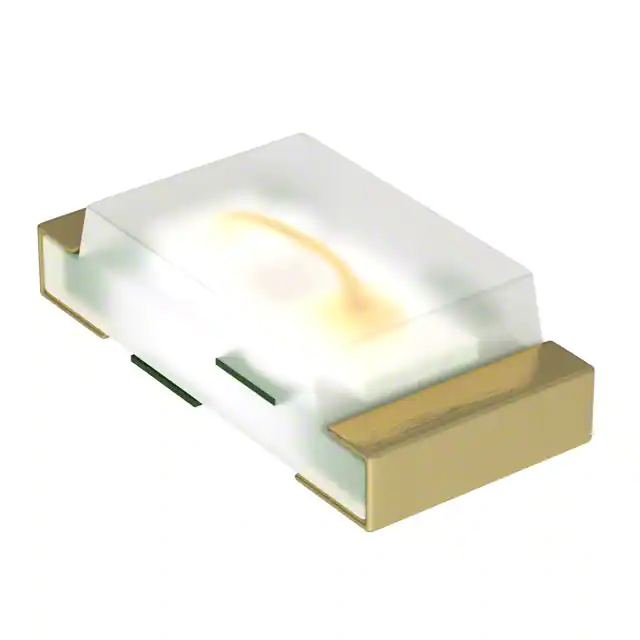
HSMW-CL25
0.25mm White Leadframe-Based Surface Mount ChipLED
Data Sheet
Description
Features
The HSMW-CL25 series of parts is designed with an ultra
small form factor to allow this miniaturization. The HSMWCL25 series is the thinnest available top emitting package
in the market with high brightness InGaN die technology.
The leadframe construction of this package allows the
part to transfer heat from the package, thus it is able to
survive temperature conditions of -40°C to 85°C despite its
small size.
• Small size top firing
The target applications are Keypad backlighting, Push
button backlighting and Status indicators.
The target markets are Mobile Handsets, Communications,
Office Automation, Industrial and Commercial
automations, Home Market appliances, Networking,
Medical Instruments, and Mobile Computing. This product
is competitively priced, and production is geared towards
short lead times and ample capacity.
• Small 1.6 (L) x 0.8 (W) x 0.25 (H) mm package
• Diffused optics
• Compatible with IR Reflow
• High brightness using InGaN die technology
• Available in 8mm Tape on 7” (178 mm) Diameter Reels
Advantages
• High package thermal dissipation capability due to the
superior package leadframe design
• Small footprint to overcome space count
• Low thickness to overcome space constrains
• Short lead times and competitive pricing
CAUTION: HSMW-CL25 LEDs are Class 1B ESD sensitive per JESD22-A114C.01. Please observe appropriate
precautions during handling and processing. Refer to Application Note AN-1142 for additional details.
�
�Package Dimensions
Notes:
1. All dimensions in millimeters (inches).
2. Tolerance is ±0.1mm (±0.004 in.) unless otherwise specified
Device Selection Guide
Package Dimension (mm)
Die Technology
Colors
Testing Current (mA)
Parts per Reel
Package Description
1.6 (L) x 0.8 (W) x 0.25 (H)
InGaN
White
5
4000
Untinted, Diffused
Absolute Maximum Ratings at TA = 25°C
Parameter
HSMW-CL25
Units
DC Forward Current[1]
10
mA
Power Dissipation
39
mW
Reverse Voltage (IR = 100mA)
5
V
LED Junction Temperature
95
°C
-40 to +85
°C
-40 to +85
°C
Operating Temperature Range
Storage Temperature Range
Soldering Temperature
Notes:
1. Derate linearly as shown in Figure 4.
�
See reflow soldering profile (Figure 7 & 8)
�Electrical Characteristics at TA = 25°C
Forward Voltage
VF (Volts) [1]
@ IF =5mA
Part Number
Typ.
Max.
Reverse Breakdown
VR (Volts) @ IR = 100mA
Min.
Thermal Resistance
RqJ-PIN (°C/W)
Typ.
HSMW-CL25
2.85
3.15
5
300
Chromaticity Coordinates[2]
Notes:
1. Vf tolerance : ±0.1V
Optical Characteristics at TA = 25°C
Luminous Intensity
IV [1] (mcd) @ 5mA
Part Number
Min.
Typ.
Bin
Viewing Angle[3] (°)
Typ.
HSMW-CL25
28.5
70.0
A1 – D2 (Refer to Figure 1)
120
Notes:
1. The luminous intensity IV is measured at the peak of the spatial radiation pattern which may not be aligned with the mechanical axis of the LED
package.
2. The chromaticity coordinates, are derived from the CIE Chromaticity Diagram and represents the perceived color of the device.
3. q1/2 is the off-axis angle where the luminous intensity is ½ the peak intensity.
Light Intensity (IV) Bin Limits
Bin ID
Forward Voltage (VF) Bin Limits
Intensity (mcd)
Bin ID
Minimum
Maximum
Minimum
Maximum
N
28.50
45.00
1
2.55
2.75
P
45.00
71.50
2
2.75
2.95
Q
71.50
112.50
3
2.95
3.15
Tolerance : ±15%
Tolerance : ±0.1V
0.38
Rank
A1
0.36
0.34
Y - COORDINATE
0.32
C1
0.30
0.28
0.26
B1
A1
0.24
0.22
D1
A2
D2
B1
B2
C2
C1
B2
A2
C2
0.20
D1
0.18
0.16
0.24
D2
0.26
0.28
0.3
X - COORDINATE
0.32
0.34
Figure 1. SMT White Color Bin Structure (CIE 1931 Chromaticity Diagram)
[Tolerance = +/- 0.02]
�
Forward Voltage (V)
X
Y
X
Y
X
Y
X
Y
X
Y
X
Y
X
Y
X
Y
Chromaticity Coordinates
0.2700
0.2700
0.2500
0.2455
0.2780
0.2500
0.2700
0.2700
0.2500
0.2455
0.2130
0.1850
0.2700
0.2700
0.2900
0.2455
0.2780
0.3060
0.2700
0.2700
0.2900
0.2455
0.2130
0.2410
0.2900
0.3100
0.3100
0.3060
0.3355
0.3030
0.2900
0.3100
0.3100
0.2410
0.2705
0.3030
0.3100
0.3100
0.3300
0.3030
0.3355
0.3650
0.3100
0.3100
0.3300
0.3030
0.2705
0.3000
0.2500
0.2175
0.2500
0.2175
0.2900
0.2735
0.2900
0.2735
0.2900
0.2735
0.2900
0.2735
0.3300
0.3325
0.3300
0.3325
�100
2.0
RELATIVE LUMINOUS INTENSITY
(NORMALIZED AT 5 mA)
FORWARD CURRENT - mA
1.8
10
1
1.6
1.4
1.2
1.0
0.8
0.6
0.4
0.2
0.1
2.0
2.5
3.0
3.5
FORWARD VOLTAGE - V
0
4.0
Figure 2. Forward voltage vs. forward current
2
4
6
8
DC FORWARD CURRENT - mA
10
Figure 3. Luminous intensity vs. forward current
12
1
0.9
NORMALIZED INTENSITY
10
RELATIVE LUMINOUS INTENSITY
(NORMALIZED AT 5 mA)
0
8
6
4
2
0.8
0.7
0.6
0.5
0.4
0.3
0.2
0.1
0
0
20
40
60
80
DC FORWARD CURRENT - mA
Figure 4. Maximum forward current vs. ambient temperature
0.8 (0.031)
0.8
(0.031)
0.7
(0.028)
0.8
(0.031)
Notes:
1. All dimensions are in millimeters (inches).
2. Tolerance is ±0.1mm (±0.004in.) unless otherwise specified.
Figure 6. Recommended soldering land pattern.
�
100
0
-90
-60
-30
0
30
60
ANGULAR DISPLACEMENT - DEGREES
Figure 5. Radiation Pattern
90
�10 SEC. MAX.
10 - 30 SEC.
255 - 260 ˚C
140-160 oC
4o C/SEC MAX.
-3o C/SEC MAX.
4o C/SEC MAX.
TEMPERATURE
TEMPERATURE
230o C MAX.
OVER 2 MIN.
217 ˚C
200 ˚C
3 ˚C/SEC. MAX.
-6 ˚C/SEC. MAX.
150 ˚C
3 ˚C/SEC. MAX.
60 - 120 SEC.
100 SEC. MAX.
TIME
TIME
Figure 7. Recommended reflow soldering profile
Figure 8. Recommended Pb-free reflow soldering profile.
USER FEED DIRECTION
PRINTED LABEL
(Acc. to J-STD-020C)
xxx
xxxxx
xxxxx
xxxxx
xxxxx
xx
CATHODE SIDE
Figure 9. Reeling orientation.
∅ 13.1 ± 0.5
(∅ 0.516 ± 0.020)
∅ 20.20 MIN.
(∅ 0.795 MIN.)
3.0 ± 0.5
(0.118 ± 0.020)
59.60 ± 1.00
(2.346 ± 0.039)
178.40 ± 1.00
(7.024 ± 0.039)
4.0 ± 0.5
(0.157 ± 0.020)
6
PS
5.0 ± 0.5
(0.197 ± 0.020)
10.50 ± 1.0 (0.413 ± 0.039)
Notes:
1. All dimensions are in millimeters (inches).
2. Tolerance is ±0.1mm (±0.004in.) unless otherwise specified.
Figure 10. Reel dimensions.
�
8.0 ± 1.0 (0.315 ± 0.039)
�DIM. A
1.75 (0.069)
± 0.10 (0.004)
PART NUMBER
HSMW-CL25
DIM. B
0.88 (0.035)
± 0.10 (0.004)
DIM. C
0.40 (0.016)
± 0.10 (0.004)
Figure 11. Tape Dimensions
END
THERE SHALL BE A
MINIMUM OF 160 mm
(6.3 INCH) OF EMPTY
COMPONENT POCKETS
SEALED WITH COVER
TAPE.
START
MOUNTED WITH
COMPONENTS
THERE SHALL BE A
MINIMUM OF 160 mm
(6.3 INCH) OF EMPTY
COMPONENT POCKETS
SEALED WITH COVER
TAPE.
Figure 12. Tape leader and trailer dimensions.
MINIMUM OF
230 mm
(9.05 INCH)
MAY CONSIST
OF CARRIER
AND/OR
COVER TAPE.
Reflow Soldering:
Storage Condition: 5 to 30°C @ 60%RH max.
For more information on reflow soldering, refer to
Application Note AN-1060, Surface Mounting SMT LED
Indicator Components.
Baking is required before mounting, if:
1. Humidity Indicator Card is > 10% when read at 23 ± 5°C.
2. Device expose to factory conditions
很抱歉,暂时无法提供与“HSMW-CL25”相匹配的价格&库存,您可以联系我们找货
免费人工找货