MGA-31389
High Gain Driver Amplifier
50MHz ~ 2GHz
Data Sheet
Description
Features
Avago Technologies MGA-31389 is a high performance
Driver Amplifier MMIC, housed in a standard SOT-89 plastic
package. The device features flat high gain with excellent
input and output return loss, as well as superior linearity
performance. The device can be easily matched to obtain
desired performance.
x� ROHS compliant
MGA-31389 is especially ideal for 50 : wireless infrastructure application within the 50 MHz to 2GHz frequency
range applications. With high IP3 and low noise figure and
wideband operation, the MGA-31389 may be utilized as
a driver amplifier in the transmit chain and as a second
stage LNA in the receiver chain.
x� Advanced enhancement mode PHEMT Technology
This device uses Avago Technologies proprietary 0.25 Pm
GaAs Enhancement mode PHEMT process.
At 0.9 GHz, Vd = 5 V, Id = 73 mA (typ) @ 25° C
x� High IP3 at low DC bias power(1)
x� High gain, with good gain flatness
x� Low noise figure
x� Excellent uniformity in product specification
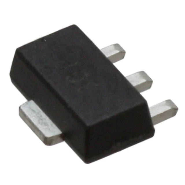
x� SOT-89 standard package
Specifications
x� OIP3 = 38.6 dBm
x� Noise Figure = 2.0 dB
Pin connections and Package Marking
GND
x� Halogen free
x� Gain = 21.3 dB, Gain flatness (± 50 MHz) = 0.14 dB
GND
x� P1dB = 22.2 dBm
x� IRL = 30.5 dB, ORL = 14.7 dB
13X
Note:
1. The MGA-31389 has a superior LFOM of 13.3 dB. Linearity Figure of
Merit (LFOM) is essentially OIP3 divided by DC bias power.
Simplified Schematic
Input
GND
Output
Output
GND
Input
Vdd
Top View
Bottom View
C
Note:
Package marking provides orientation and identification
“13” = Device Code
“X” = Date Code character indentifies month of manufacturing
Attention: Observe precautions for
handling electrostatic sensitive devices.
ESD Machine Model = 75 V
ESD Human Body Model = 1000 V
Refer to Avago Application Note A004R:
Electrostatic Discharge, Damage and Control.
C
C
L
RFout
RFin
C
Figure 1. Simplified Schematic diagram
C
�MGA-31389 Absolute Maximum Rating (1) TA=25° C
Thermal Resistance
Symbol
Parameter
Units
Absolute Max.
Vd, max
Drain Voltage, RF output to ground
V
5.5
Pd
Power Dissipation (2)
mW
605
Pin
CW RF Input Power
dBm
20
Tj
Junction Temperature
°C
150
TSTG
Storage Temperature
°C
-65 to 150
Thermal Resistance (3)
(Vd = 5.0 V, Tc = 85° C), Tjc = 60.0° C/W
Notes:
1. Operation of this device in excess of any of
these limits may cause permanent damage.
2. Source lead temperature is 25° C. Derate 16.7
mW/° C for TL>128.0° C.
3. Thermal resistance measured using 150° C
Infra-Red Microscopy Technique.
MGA-31389 Electrical Specification (1)
TC = 25° C, Vd = 5 V, unless noted
Symbol
Parameter and Test Condition
Frequency
Units
Min.
Typ.
Max.
Ids
Quiescent Current
N/A
mA
62
73
90
NF
Noise Figure
0.45 GHz
0.9 GHz
1.5 GHz
dB
–
2.3
2.0
2.0
2.5
0.45 GHz
0.9 GHz
1.5 GHz
dB
20
21.5
21.3
20.6
23
0.45 GHz (2)
0.9 GHz (2)
1.5 GHz (2)
dBm
36.3
38.6
38.6
41.3
–
0.45 GHz
0.9 GHz
1.5 GHz
dBm
20.6
22.0
22.2
21.7
–
0.45 GHz
0.9 GHz
1.5 GHz
%
–
41.0
41.2
38.4
–
0.45 GHz
0.9 GHz
1.5 GHz
dB
–
24.3
30.5
15.3
–
0.45 GHz
0.9 GHz
1.5 GHz
dB
–
11.4
14.7
12.1
–
0.45 GHz
0.9 GHz
1.5 GHz
dB
–
27.2
27.6
28.6
–
Gain
OIP3 (2)
P1dB
PAE
IRL
ORL
ISOL
Gain
Output Third Order Intercept Point
Output Power at 1 dB Gain Compression
Power Added Efficiency at P1dB
Input Return Loss
Output Return Loss
Isolation
Note :
1. Measurements obtained from a test circuit described in Figure 34
2. OIP3 test condition: F1 - F2 = 10 MHz, with input power of -14 dBm per tone measured at worst case side band.
2
�MGA-31389 Consistency Distribution Chart (1,2)
70
80
1.7
Figure 2. Id @ 900MHz, Vd=5V, LSL=62mA, Nominal=76mA, USL=90mA
20.8
21 21.1
21.3
21.5
21.7
21.9 22 22.1
Figure 4. Gain @ 900MHz, Vd=5V, LSL=20dB, Nominal=21.5dB, USL=23dB
1.8
1.8
2
2.1
2.2
2.3
Figure 3. NF @ 900MHz, Vd=5V, Nominal=2.0dB, USL=2.5dB
38
39
40
41
Figure 5. OIP3 @ 900MHz, Vd=5V, LSL=36.3dBm, Nominal=39.3dBm
21
22
23
Figure 6. P1dB @ 900MHz, Vd=5V, LSL= 20.6dBm, Nominal=22.2dBm
Notes:
1. Data sample size is 3000 samples taken from 3 different wafers and 2 different lots. Future wafers allocated to this product may have nominal
values anywhere between the upper and lower limits.
2. Measurements are made on production test board which represents a trade-off between optimal Gain, NF, OIP3 and OP1dB. Circuit losses have
been de-embedded from actual measurements.
3
�MGA-31389 Application Circuit Data for 450 MHz
23
44
43
42
41
40
39
38
37
36
35
34
33
22
P1dB (dBm)
OIP3 (dBm)
Tc = 25° C, Vd = 5.0 V, Id = 73 mA
25° C
-40° C
85° C
150
250
350
450
550
Frequency (MHz)
650
22
-5
21
-10
18
350
450
550
Frequency (MHz)
650
250
350
450
550
Frequency (MHz)
750
25° C
-40° C
85° C
650
-20
-25
-30
25° C
-40° C
85° C
17
-35
-40
150
750
Figure 9. Gain vs Frequency and Temperature
250
350
450
550
Frequency (MHz)
650
750
Figure 10. IRL vs Frequency and Temperature
-26
0
25° C
-40° C
85° C
-27
Isolation (dB)
-5
-10
-15
-20
-25
150
250
-15
19
16
150
25° C
-40° C
85° C
Figure 8. P1dB vs Frequency and Temperature
IRL (dB)
Gain (dB)
19
17
150
750
20
ORL (dB)
20
18
Figure 7. OIP3 vs Frequency and Temperature
-28
-29
25° C
-40° C
85° C
-30
250
350
450
550
Frequency (MHz)
Figure 11. ORL vs Frequency and Temperature
4
21
650
750
-31
150
250
350
450
550
Frequency (MHz)
Figure 12. Isolation vs Frequency and Temperature
650
750
�MGA-31389 Application Circuit Data for 450 MHz (cont'd)
Tc = 25° C, Vd = 5.0 V, Id = 73 mA
3.0
2.0
OIP3 (dBm)
Noise Figure (dB)
2.5
1.5
1.0
25° C
-40° C
85° C
0.5
0.0
150
250
350
450
550
Frequency (MHz)
650
750
Figure 13. Noise Figure vs Frequency and Temperature
25° C
-40° C
85° C
0.0 0.5 1.0 1.5 2.0 2.5 3.0 3.5 4.0 4.5 5.0 5.5
Voltage (Volt)
Figure 15. Current vs Voltage and Temperature
5
25° C
-40° C
85° C
-20 -19 -18 -17 -16 -15 -14 -13 -12 -11 -10 -9 -8 -7 -6 -5
Pin (dBm)
Figure 14. OIP3 vs Input Power and Temperature
Current (mA)
110
100
90
80
70
60
50
40
30
20
10
0
43
42
41
40
39
38
37
36
35
34
33
32
31
30
29
�MGA-31389 Application Circuit Data for 900 MHz
50
49
48
47
46
45
44
43
42
41
40
39
38
37
36
35
600
23.0
25° C
-40° C
85° C
22.5
P1dB (dBm)
OIP3 (dBm)
Tc = 25° C, Vd = 5.0 V, Id = 73 mA
22.0
21.5
21.0
25° C
-40° C
85° C
20.5
20.0
700
800
900
1000
Frequency (MHz)
1100
1200
Figure 16. OIP3 vs Frequency and Temperature
600
700
800
900
1000
Frequency (MHz)
1100
1200
1100
1200
Figure 17. P1dB vs Frequency and Temperature
22.0
-10
21.5
-15
IRL (dB)
Gain (dB)
21.0
20.5
-20
-25
20.0
25° C
-40° C
85° C
19.5
19.0
600
700
800
900
1000
Frequency (MHz)
1100
-35
600
1200
Figure 18. Gain vs Frequency and Temperature
700
800
900
1000
Frequency (MHz)
Figure 19. IRL vs Frequency and Temperature
0
-27.0
25° C
-40° C
85° C
-5
-27.5
Isolation (dB)
-10
ORL (dB)
25° C
-40° C
85° C
-30
-15
-20
-25
-28.0
-28.5
25° C
-40° C
85° C
-30
-35
600
700
800
900
1000
Frequency (MHz)
Figure 20. ORL vs Frequency and Temperature
6
1100
1200
-29.0
600
700
800
900
1000
Frequency (MHz)
Figure 21. Isolation vs Frequency and Temperature
1100
1200
�MGA-31389 Application Circuit Data for 900 MHz (cont'd)
Tc = 25° C, Vd = 5.0 V, Id = 73 mA
3.0
2.0
OIP3 (dBm)
Noise Figure (dB)
2.5
1.5
1.0
25° C
-40° C
85° C
0.5
0.0
600
700
800
900
1000
Frequency (MHz)
1100
1200
Figure 22. Noise Figure vs Frequency and Temperature
25° C
-40° C
85° C
0.0 0.5 1.0 1.5 2.0 2.5 3.0 3.5 4.0 4.5 5.0 5.5
Voltage (Volt)
Figure 24. Current vs Voltage and Temperature
7
25° C
-40° C
85° C
-20 -19 -18 -17 -16 -15 -14 -13 -12 -11 -10 -9 -8 -7 -6 -5
Pin (dBm)
Figure 23. OIP3 vs Input Power and Temperature
Current (mA)
110
100
90
80
70
60
50
40
30
20
10
0
43
42
41
40
39
38
37
36
35
34
33
32
31
30
�MGA-31389 Application Circuit Data for 1500MHz
Tc = 25° C, Vd = 5.0 V, Id = 73 mA
44
23.0
25° C
-40° C
85° C
43
22.5
41
P1dB (dBm)
OIP3 (dBm)
42
40
39
22.0
21.5
21.0
38
36
1200
1300
1400
1500
1600
Frequency (MHz)
1700
20.0
1200
1800
Figure 25. OIP3 vs Frequency and Temperature
IRL (dB)
Gain (dB)
20.5
20.0
19.5
25° C
-40° C
85° C
1300
1400
1500
1600
Frequency (MHz)
1700
1800
Figure 27. Gain vs Frequency and Temperature
1800
-10
-11
-12
-13
-14
-15
-16
-17
-18
-19
-20
1200
25° C
-40° C
85° C
1300
1400
1500
1600
Frequency (MHz)
1700
1800
-28.0
Isolation (dB)
ORL (dB)
1700
-27.5
25° C
-40° C
85° C
-5
-10
-28.5
-29.0
-15
1300
1400
1500
1600
Frequency (MHz)
Figure 29. ORL vs Frequency and Temperature
8
1400
1500
1600
Frequency (MHz)
Figure 28. IRL vs Frequency and Temperature
0
-20
1200
1300
Figure 26. P1dB vs Frequency and Temperature
21.0
19.0
1200
25° C
-40° C
85° C
20.5
37
1700
1800
-29.5
1200
25° C
-40° C
85° C
1300
1400
1500
1600
Frequency (MHz)
Figure 30. Isolation vs Frequency and Temperature
1700
1800
�MGA-31389 Application Circuit Data for 1500 MHz (cont'd)
Tc = 25° C, Vd = 5.0 V, Id = 73 mA
3.0
2.0
OIP3 (dBm)
Noise Figure (dB)
2.5
1.5
1.0
25° C
-40° C
85° C
0.5
0.0
1200
1300
1400
1500
1600
Frequency (MHz)
1700
1800
Figure 31. Noise Figure vs Frequency and Temperature
25° C
-40° C
85° C
0.0 0.5 1.0 1.5 2.0 2.5 3.0 3.5 4.0 4.5 5.0 5.5
Voltage (Volt)
Figure 33. Current vs Voltage and Temperature
9
25° C
-40° C
85° C
-20 -19 -18 -17 -16 -15 -14 -13 -12 -11 -10 -9 -8 -7 -6 -5
Pin (dBm)
Figure 32. OIP3 vs Input Power and Temperature
Current (mA)
110
100
90
80
70
60
50
40
30
20
10
0
44
43
42
41
40
39
38
37
36
35
34
33
32
31
30
29
28
�Application Circuit Description and Layout
Vdd
C3
C2
C1
13X
L1
RFout
RFin
C7
C8
Figure 34. Circuit diagram
Figure 35. Demoboard
Bill of Materials
Description
For 0.45 GHz (1)
For 0.9 GHz (2)
For 1.5 GHz (3)
Circuit
Symbol
Size
Value
Manufacturer
Value
Manufacturer
Value
Manufacturer
C1
0402
10 pF
Murata
3.0 pF
Murata
3.9 pF
Murata
C2
0402
0.1 PF
Murata
0.1 PF
Murata
0.1 PF
Murata
C3
0603
2.2 PF
Murata
2.2 PF
Murata
2.2 PF
Murata
C7
0402
100 pF
Murata
100 pF
Murata
100 pF
Murata
C8
0402
15 pF
Murata
5.6 pF
Murata
3 pF
Murata
L1
0402
39 nH
Murata
12 nH
Murata
3.9 nH
Murata
DCin
RFin
Input Matching Circuit
1. *_mag = 0.055, G_ang = -94.4°
2. *_mag = 0.070, G_ang = -98.9°
3. *_mag = 0.095, G_ang = -117.1°
13X
Output Matching Circuit
1. *_mag = 0.066, G_ang = -21.4°
2. *_mag = 0.152, G_ang = 15.1°
3. *_mag = 0.275, G_ang = 60.1°
RFout
Figure 36. Input and output tuned Gamma location for 450MHz (1), 900MHz (2) and 1500MHz (3)
For best performance, MGA-31389 is an input and output prematched driver amplifier. To bias MGA-31389, a +5V supply
(Vdd) is connected to the output pin through a RF choke, L1 (which isolates the inband signal from the DC supply). The
bypass capacitor helps to eliminate out of low band frequency signals from the power supply, C3, C2 and C1. Blocking
capacitors are required for its input (C7) and output (C8), to isolate the supply voltage from preceeding and succeeding circuits. C7 also plays a part in input tuning to improve input return loss while L1 and C8 help in tuning output. The
recommended output tuning is for achieving best OIP3, while meeting typical specifications for other parameters.
10
�MGA-31389 Typical Scatter Parameters (1)
Tc = 25° C, Vd = 5.0 V, Id = 73 mA, Zo = 50 :
Freq
GHz
S11
Mag.
S11
dB
S11
Ang.
S21
Mag.
S21
dB
S21
Ang.
S12
Mag.
S12
dB
S12
Ang.
S22
Mag.
S22
dB
S22
Ang.
K Factor
0.10
0.046
-26.7
-127.5
12.372
21.8
169.8
0.046
-26.8
-3.3
0.281
-11.0
172.9
1.100
0.20
0.034
-29.4
-146.1
12.409
21.9
162.4
0.046
-26.7
-9.9
0.270
-11.4
160.6
1.104
0.30
0.032
-29.9
-150.7
12.415
21.9
154.2
0.046
-26.7
-15.9
0.258
-11.8
149.5
1.108
0.40
0.035
-29.0
-146.0
12.406
21.9
145.8
0.046
-26.8
-21.9
0.240
-12.4
138.9
1.117
0.50
0.040
-27.9
-138.6
12.386
21.9
137.2
0.046
-26.8
-27.8
0.216
-13.3
128.8
1.130
0.60
0.047
-26.5
-135.8
12.350
21.8
128.6
0.045
-26.9
-33.7
0.189
-14.5
118.3
1.143
0.70
0.053
-25.5
-137.3
12.308
21.8
119.8
0.045
-27.0
-39.6
0.161
-15.9
107.3
1.158
0.80
0.057
-24.8
-141.8
12.247
21.8
111.1
0.044
-27.0
-45.6
0.133
-17.5
95.1
1.174
0.90
0.059
-24.5
-149.0
12.179
21.7
102.2
0.044
-27.2
-51.5
0.106
-19.5
81.1
1.192
1.00
0.058
-24.8
-158.8
12.092
21.7
93.4
0.043
-27.3
-57.6
0.081
-21.8
63.4
1.211
1.10
0.051
-25.8
-168.3
12.003
21.6
84.5
0.043
-27.4
-63.3
0.067
-23.5
39.1
1.230
1.20
0.042
-27.6
170.5
11.913
21.5
75.4
0.042
-27.5
-69.2
0.054
-25.3
10.9
1.248
1.30
0.035
-29.1
131.7
11.805
21.4
66.2
0.041
-27.7
-75.2
0.049
-26.3
-21.3
1.266
1.40
0.042
-27.5
83.8
11.686
21.4
56.9
0.041
-27.8
-81.2
0.052
-25.7
-53.4
1.282
1.50
0.067
-23.5
50.5
11.545
21.2
47.4
0.040
-27.9
-87.4
0.060
-24.4
-78.5
1.298
1.60
0.102
-19.9
28.8
11.382
21.1
37.7
0.040
-28.0
-93.6
0.070
-23.1
-98.5
1.311
1.70
0.143
-16.9
12.1
11.165
21.0
27.8
0.039
-28.2
-100.3
0.080
-22.0
-114.8
1.324
1.80
0.189
-14.5
-2.8
10.908
20.8
17.9
0.039
-28.3
-107.1
0.089
-21.0
-128.9
1.335
1.90
0.240
-12.4
-16.6
10.600
20.5
7.7
0.038
-28.4
-114.4
0.096
-20.3
-141.7
1.348
2.00
0.292
-10.7
-30.0
10.230
20.2
-2.5
0.037
-28.6
-121.8
0.102
-19.8
-153.3
1.364
2.10
0.346
-9.2
-43.5
9.831
19.9
-12.8
0.036
-28.8
-129.5
0.107
-19.4
-164.5
1.384
2.20
0.398
-8.0
-56.6
9.365
19.4
-23.1
0.035
-29.1
-137.6
0.108
-19.3
-175.7
1.411
2.30
0.450
-6.9
-69.7
8.862
19.0
-33.4
0.034
-29.4
-145.7
0.107
-19.4
174.4
1.447
2.40
0.501
-6.0
-82.4
8.323
18.4
-43.6
0.033
-29.7
-154.1
0.104
-19.7
165.1
1.489
2.50
0.549
-5.2
-94.7
7.764
17.8
-53.5
0.031
-30.1
-162.4
0.098
-20.1
156.7
1.546
3.00
0.744
-2.6
-148.3
5.017
14.0
-99.1
0.023
-32.8
157.6
0.040
-27.9
148.5
1.973
3.50
0.853
-1.4
174.9
3.042
9.7
-135.2
0.017
-35.6
124.7
0.089
-21.0
-133.1
2.645
4.00
0.900
-0.9
150.2
1.908
5.6
-163.5
0.014
-37.2
98.7
0.195
-14.2
-142.0
3.446
5.00
0.908
-0.8
105.9
0.945
-0.5
147.1
0.014
-37.2
55.9
0.328
-9.7
-167.2
6.072
6.00
0.903
-0.9
41.9
0.502
-6.0
91.2
0.016
-36.0
9.0
0.340
-9.4
156.6
10.230
7.00
0.943
-0.5
-1.6
0.240
-12.4
42.9
0.015
-36.5
-28.8
0.431
-7.3
112.4
12.763
8.00
0.958
-0.4
-16.7
0.131
-17.7
5.7
0.014
-37.1
-55.2
0.509
-5.9
71.7
16.973
9.00
0.938
-0.6
-38.6
0.082
-21.8
-33.5
0.013
-37.9
-83.4
0.546
-5.3
29.8
40.810
10.00
0.941
-0.5
-75.0
0.045
-26.9
-76.8
0.009
-41.2
-117.9
0.610
-4.3
-16.1
92.313
11.00
0.961
-0.3
-101.8
0.020
-33.8
-108.6
0.003
-49.3
-143.7
0.740
-2.6
-49.3
245.787
12.00
0.974
-0.2
-116.2
0.009
-41.4
-122.2
0.000
-68.3
-14.2
0.824
-1.7
-66.2
2552.738
13.00
0.969
-0.3
-127.3
0.004
-49.0
-108.5
0.003
-49.4
-6.7
0.839
-1.5
-85.5
746.065
14.00
0.951
-0.4
-145.5
0.004
-48.2
-63.1
0.006
-43.8
-28.7
0.836
-1.6
-115.5
573.063
15.00
0.956
-0.4
-168.7
0.006
-44.3
-70.1
0.008
-41.9
-57.1
0.871
-1.2
-144.7
211.605
16.00
0.966
-0.3
178.6
0.006
-45.1
-101.7
0.007
-43.5
-89.3
0.910
-0.8
-158.6
153.352
17.00
0.966
-0.3
171.8
0.002
-53.8
-69.5
0.003
-49.9
-64.3
0.924
-0.7
-162.9
749.036
18.00
0.949
-0.5
158.3
0.004
-49.1
-14.3
0.004
-47.2
-27.6
0.906
-0.9
-170.2
587.481
19.00
0.946
-0.5
139.4
0.007
-42.5
-13.5
0.008
-42.1
-21.2
0.852
-1.4
171.1
244.925
20.00
0.947
-0.5
125.2
0.012
-38.7
-17.0
0.012
-38.7
-21.6
0.822
-1.7
145.1
122.769
11
�MGA-31389 K-Factor (1)
K Factor
Tc = 25° C, Vd = 5.0 V, Id = 73 mA, Zo = 50 :
10
9
8
7
6
5
4
3
2
1
0
K Factor
0
2
4
6
8
10 12
Frequency (GHz)
14
16
18
20
MGA-31389 Typical Noise Parameters (1)
Tc = 25° C, Vd = 5.0 V, Id = 73 mA, Zo = 50 :
Freq
(GHz)
Fmin
(dB)
*opt
Mag
*opt
Ang
Rn/Z0
Ga
(dB)
0.5
2.08
0.204
4.8
0.34
22.11
0.8
1.85
0.247
20.6
0.33
21.73
0.9
1.71
0.312
6.2
0.36
21.44
1
1.75
0.309
18.7
0.36
21.38
1.5
1.90
0.264
20.6
0.31
21.06
2
2.24
0.254
90.3
0.28
20.27
2.5
2.35
0.470
118.8
0.28
18.99
3
2.88
0.601
157.6
0.13
16.91
3.5
3.53
0.714
-173.1
0.08
14.77
4
5.03
0.769
-148.1
0.49
12.19
4.5
7.91
0.855
-124.3
3.88
10.11
5
7.65
0.883
-103.0
7.78
7.38
5.5
8.82
0.868
-80.5
18.35
4.51
6
10.27
0.929
-56.6
41.09
2.21
Note:
1. Measurements are made using 10 mils Rogers RO4350 TRL Board.
12
�Package Dimensions
Dimensions are in mm
D
A
D1
C
E
H
#1
#2
E1
#3
B
L
B1
e
#3
#2
#1
e1
BOTTOM
S
Y
M
B
O
L
COMMON
A
DIMENSIONS MILLIMETER
MAX.
MIN.
NOM.
1.50
1.60
1.40
DIMENSIONS INCH
NOM.
MAX.
MIN.
0.059
0.063
0.055
B
0.44
0.50
0.56
0.017
0.0195
0.022
B1
0.36
0.42
0.48
0.014
0.0165
0.019
C
0.35
0.40
0.44
0.014
0.016
0.017
D
4.40
4.50
4.60
0.173
0.177
0.181
D1
1.62
1.73
1.83
0.064
0.068
0.072
E
2.30
2.50
2.60
0.090
0.096
0.102
E1
2.13
2.20
2.29
0.084
0.087
0.090
1.50 BSC
e
0.059 BSC
3.00 BSC
e1
0.118 BSC
H
3.95
4.10
4.25
0.155
0.161
0.167
L
0.90
1.10
1.20
0.035
0.038
0.047
M
2.36
2.46
2.56
0.093
0.097
0.101
Part Number Ordering Information
Part Number
No. of Devices
Container
MGA-31389-BLKG
100
Antistatic Bag
MGA-31389-TR1G
3000
13" Tape/Reel
13
Note :
a) Dimensioning and tolerancing per ANSI.Y14.5M-1982
b) Controlling dimension: Millimeter conversions to inches are not
necessarily exact
c) Dimension B1, 2 places.
�Device Orientation
REEL
13X
13X
13X
CARRIER
TAPE
USER FEED
DIRECTION
COVER TAPE
Tape Dimensions
8.00±0.10
(0.315±0.004)
4.00±0.10
(0.157±0.004)
2.00±0.05
(0.069±0.004)
Ø1.50±0.10
(0.059±0.004)
1.75±0.10
(0.069±0.004)
5.50±0.05
(0.217±0.002)
12.0±0.30–0.10
(0.472+0.012–0.004)
Ø1.50±0.25
(0.059±0.010)
0.292±0.02
(0.0115±0.0008)
8°
4.80±0.10
(0.180±0.004)
Dimensions in mm (inches)
14
0.180±0.10
(0.070±0.004)
6° MAX
4.40±0.10
(0.1732±0.004)
13X
�Reel Dimension – 13” Reel 12mm Width
11
12 1
2
3
4
0 2
10
9
7
6
5
DATE CODE
12MM
8
EMBOSSED LETTERING
16.0mm HEIGHT x MIN. 0.4mm THICK.
Ø329.0±1.0
HUB
Ø100.0±0.5
6
PS
0 2
1
1112 2
3
10
4
9
8 7 6 5
MP
N
CPN
EMBOSSED LETTERING
7.5mm HEIGHT
EMBOSSED LETTERING
7.5mm HEIGHT
1.5
(MI
N.)
FRONT VIEW
EMBOSSED LINE (2x)
89.0mm LENGTH LINES 147.0mm
AWAY FROM CENTER POINT
+0.5
-0.2
20.2(MIN.)
Ø13.0
11.9-15.4**
+2.0*
12.4
-0.0
Ø16.0
ESD LOGO
6
PS
RECYCLE LOGO
Detail "X"
SEE DETAIL "X"
Ø100.0±0.5
Ø329.0±1.0
6
PS
R19.0±0.5
BACK VIEW
SLOT
5.0±0.5(3x)
Ø12.3±0.5(3x)
For product information and a complete list of distributors, please go to our web site:
18.4 MAX.*
www.avagotech.com
Avago, Avago Technologies, and the A logo are trademarks of Avago Technologies in the United States and other countries.
Data subject to change. Copyright © 2005-2010 Avago Technologies. All rights reserved.
AV02-2586EN - August 11, 2010
�