MGA-631P8
Low Noise, High Linearity, Active Bias Low Noise Amplifier
Data Sheet
Description
Features
Avago Technologies’ MGA-631P8 is an economical, easyto-use GaAs MMIC Low Noise Amplifier (LNA) with active
bias. The LNA has low noise with excellent input return
loss and high linearity achieved through the use of
Avago Technologies’ proprietary 0.5um GaAs Enhancement-mode pHEMT process. The LNA has an extra feature
that allows a designer to adjust supply current and gain
externally. Due to the high isolation between the input
and output, gain can be adjusted independently through
a resistor in series with a blocking capacitor from the
output pin to FB1 pin, without affecting the noise figure.
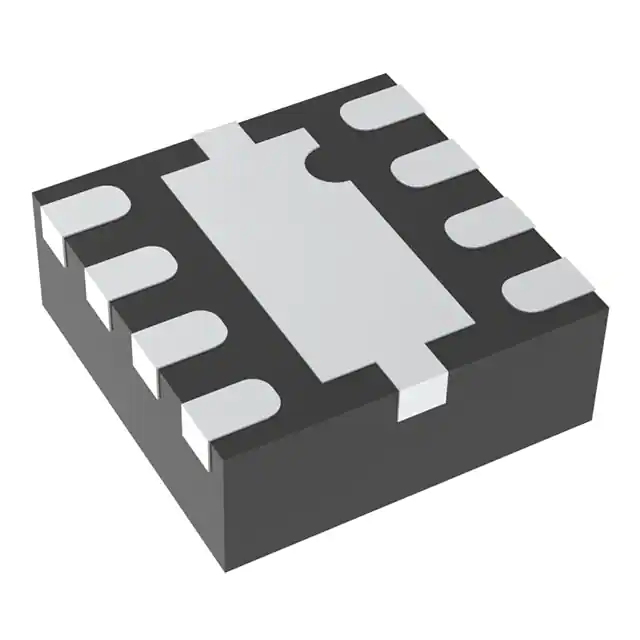
It is housed in a miniature 2.0 x 2.0 x 0.75mm3 8-pin Thin
Small Leadless Package (TSLP) package. The compact
footprint and low profile coupled with low noise, high
gain, excellent input return loss and high linearity make
the MGA-631P8 an ideal choice as an LNA for cellular infrastructure for GSM, CDMA, GPS and ISM applications.
x
x
x
x
x
x
x
It is designed for optimum use between 400MHz to
1.5GHz. For optimum performance at higher frequency
from 1.4GHz to 3.8GHz, the MGA-632P8 is recommended. Both MGA-631P8 and MGA-632P8 share the same
package and pinout.
Pin Configuration and Package Marking
Low noise figure
Good input return loss
High linearity performance
High Isolation
Externally adjustable supply current, 40-80mA
Externally adjustable gain, 15-20dB
GaAs E-pHEMT Technology[1]
x Low cost small package size: 2.0x2.0x0.75 mm3
x Excellent uniformity in product specifications
Specifications
900MHz; 4V, 54mA (typ)
x
x
x
x
x
x
17.5 dB Gain
0.53 dB Noise Figure
-19.4dB S11
-34dB S12
32.6 dBm Output IP3
18.0 dBm Output Power at 1dB gain compression
Applications
2.0 x 2.0 x 0.75 mm3 8-lead TSLP
x Low noise amplifier for cellular infrastructure for GSM,
CDMA, GPS and ISM.
x Other ultra low noise applications.
Note:
1. Enhancement mode technology employs positive Vgs, thereby
eliminating the need of negative gate voltage associated with
conventional depletion mode devices.
Top View
Bottom View
Note:
Package marking provides
orientation and identification
“G1” is Device Code
“X” is month code
Note:
Pin 1 : not used
Pin 2 : RFin
Pin 3 : RF ground
Pin 4 : Vbias
Attention: Observe precautions for
handling electrostatic sensitive devices.
ESD Machine Model = 50 V
ESD Human Body Model = 200 V
Pin 5 : FB1
Pin 6 : not used
Pin 7 : RFout
Pin 8 : Gnd
Refer to Avago Application Note A004R:
Electrostatic Discharge, Damage and Control.
�MGA-631P8 Absolute Maximum Rating [1]
Symbol
Parameter
Units
Absolute Max.
Vd
Device Supply Voltage
V
5.5
Pin,max
CW RF Input Power (Vd=4.0V, Vbias=4.0V)
dBm
20
Pdiss
Total Power Dissipation [2]
W
0.55
Tj
Junction Temperature
°C
150
TSTG
Storage Temperature
°C
-65 to 150
Thermal Resistance [3] (Vd = 4.0V, Vbias=4.0V), θJC = 47 °C/W
Notes:
1. Operation of this device in excess of any of these limits may cause permanent damage.
2. Board temperature TB is 25 °C. Derate 21.2mW/ °C for TB>124 °C.
3. Thermal resistance measured using Infra-Red Microscopy Technique.
Product Consistency Distribution Charts [4]
Process Capability for Gain
Process Capability for NF
300
Nominal = 0.53,
USL = 1.0
120
Frequency
Frequency
CPK Lower = 3.72
CPK Upper = 3.85
Std Dev = 0.13
LSL = 16.0,
Nominal = 17.5,
USL = 19.0
250
150
200
150
100
CPK=4.04
Std Dev=0.04
90
60
30
50
0
16
16.5
17
17.5 18
Gain (dB)
18.5
0
0.41
19
0.51
0.61
0.71
NF (dB)
Figure 1. Gain distribution at 54mA
CPK Lower = 2.45
CPK = 2.68
Std Dev = 1.26
LSL = 41,
Nominal = 54,
USL = 67
250
500
CPK Lower = 1.550
Std Dev = 0.369
400
Count
200
Count
Nominal = 32.6
LSL = 30.8
150
300
100
200
50
100
40
45
50
55
60
Id (mA)
Figure 3. Id distribution at 54mA
65
70
31
32
33
OIP3U (dBm)
34
35
Figure 4. OIP3U distribution at 54mA
4. Distribution data sample size is 500 samples taken from 3 different wafer lots. Future wafer allocated to this product may have nominal values
anywhere between the upper and lower limits. Circuit losses have been de-embedded from actual measurements.
2
�Electrical Specifications [1,2]
TA = 25 °C, Vd =4V @ 54mA, R1=91ohm unless otherwise specified.
Symbol
Parameter and Test Condition
Units
Min.
Typ.
Max.
41
54
67
16.0
18.4
17.9
17.5
19.0
30.8
34.2
33.8
32.6
Id
Operational Current
Vbias=4.0V
mA
Gain
Freq=800 MHz
Freq=850 MHz
Freq=900 MHz
Associated Gain
dB
OIP3
Freq=800 MHz
Freq=850 MHz
Freq=900 MHz
Output Third Order Intercept Point
(2-tone @ FRF +/- 5MHz, Pin = -20dBm)
dBm
Freq=800 MHz
Freq=850 MHz
Freq=900 MHz
Noise Figure in 50: system
OP1dB
Freq=800 MHz
Freq=850 MHz
Freq=900 MHz
Output Power at 1dB Gain Compression
dBm
18.3
18.0
18.0
IRL
Freq=800 MHz
Freq=850 MHz
Freq=900 MHz
Input Return Loss
dB
-20.9
-30.6
-19.4
ORL
Freq=800 MHz
Freq=850 MHz
Freq=900 MHz
Output Return Loss
dB
-21.3
-22.1
-22.5
S12
Freq=800 MHz
Freq=850 MHz
Freq=900 MHz
Reverse Isolation
dB
-34.0
-34.0
-34.0
NF50Ω
dB
0.57
0.51
0.53
1.0
Notes:
1. Measurements obtained using demo board described in Figure 28 and Table 1, List 1. Input and output board losses have been de-embedded.
2. Guaranteed specifications are 100% tested in production test circuit.
Typical Electrical Specifications at 700MHz [3]
TA = 25 °C, Vd =4V @ 54mA, R1=91ohm unless otherwise specified.
Symbol
Parameter and Test Condition
Units
Typ.
Gain
Freq=700MHz
Associated Gain
dB
17.1
OIP3
Freq=700MHz
Output Third Order Intercept Point
(2-tone @ FRF +/- 5MHz, Pin = -20dBm)
dBm
35.7
NF50Ω
Freq=700MHz
Noise Figure in 50: system
dB
1.12
OP1dB
Freq=700MHz
Output Power at 1dB Gain Compression
dBm
15.1
IRL
Freq=700MHz
Input Return Loss
dB
-12.1
ORL
Freq=700MHz
Output Return Loss
dB
-3.2
S12
Freq=700MHz
Reverse Isolation
dB
-38.4
Notes:
3. Measurements obtained using demo board described in Figure 28 and Table 1, List 4. Input and output board losses have been de-embedded.
3
�MGA-631P8 Typical Performance[1]
TA = 25 °C, Vd = 4V, Id = 54mA, R1=91ohm unless stated otherwise.
1
21
0.9
19
0.8
17
0.7
0.6
NF (dB)
Gain (dB)
15
13
0.5
0.4
11
0.3
9
20mA
40mA
60mA
80mA
7
5
780
800
820
840
860
Frequency (MHz)
880
20mA
40mA
60mA
80mA
0.2
0.1
900
0
780
920
Figure 5. Gain Vs Frequency and Id
800
820
840
860
Frequency (MHz)
880
900
920
Figure 6. NF Vs Frequency and Id
20
40
18
16
30
14
25
12
Gain (dB)
OIP3 (dBm)
35
20
10
15
8
6
20mA
40mA
60mA
80mA
10
5
0
780
3V Vd
4V Vd
5V Vd
4
2
0
800
820
840
860
Frequency (MHz)
880
900
10
920
20
30
40
50
Id (mA)
60
70
80
90
Figure 8. Gain Vs Id and Vd
Figure 7. OIP3 Vs Frequency and Id
1
40
0.9
35
0.8
30
0.7
25
OIP3 (dBm)
NF (dB)
0.6
0.5
0.4
20
15
0.3
0.2
10
3V Vd
4V Vd
5V Vd
0.1
0
10
20
30
Figure 9. NF Vs Id and Vd
40
50
Id (mA)
60
70
80
3V Vd
4V Vd
5V Vd
5
90
0
10
20
40
Figure 10. OIP3 Vs Id and Vd
Notes:
1. Measurements obtained using demo board described in Figure 28 and Table 1, List 1.
4
30
50
Id (mA)
60
70
80
90
�MGA-631P8 Typical Performance[1]
TA = 25 °C, Vd = 4V, Id = 54mA, R1=91ohm unless stated otherwise.
19
70
18
60
17
16
40
Gain (dB)
Id (mA)
50
30
14
13
20
0
1
2
3
4
Vd (V)
5
6
-40°C
25°C
85°C
12
-40°C
85°C
25°C
10
0
15
11
7
10
780
8
Figure 11. Id Vs Vd and Temperature
800
820
840
860
Frequency (MHz)
880
900
920
Figure 12. Gain Vs Frequency and Temperature
0.8
40
0.7
35
0.6
30
OIP3 (dBm)
NF (dB)
0.5
25
0.4
0.3
20
-40°C
-30°C
25°C
85°C
0.2
-40°C
25°C
85°C
0.1
0.0
780
800
820
840
860
880
Frequency (MHz)
900
15
920
Figure 13. NF Vs Frequency and Temperature
10
780
800
820
840
860
Frequency (MHz)
880
900
920
Figure 14. OIP3 vs Frequency and Temperature
20
0.8
18
0.7
16
0.6
0.5
12
NF (dB)
Gain (dB)
14
10
8
0.4
0.3
6
0.2
-40°C
25°C
85°C
4
2
0
10
20
30
40
50
Id (mA)
Figure 15. Gain vs Id and Temperature
60
70
80
90
0.0
10
20
30
40
50
Id (mA)
Figure 16. NF Vs Id and Temperature
Notes:
1. Measurements obtained using demo board described in Figure 28 and Table 1, List 1.
5
-40°C
25°C
85°C
0.1
60
70
80
90
�MGA-631P8 Typical Performance[1]
TA = 25 °C, Vd = 4V, Id = 54mA, R1=91ohm unless stated otherwise.
40
25
35
20
25
15
Gain (dB)
OIP3 (dBm)
30
20
15
10
-40°C
-30°C
25°C
85°C
5
20
30
40
50
Id (mA)
60
70
80
R1=56ohms
R1=91ohms
R1=560ohms
5
0
780
0
10
10
90
Figure 17. OIP3 vs Id and Temperature
800
820
840
860
880
Frequency (MHz)
900
920
Figure 18. Gain Vs Frequency and R1
40
1
R1=56ohms
R1=91ohms
R1=560ohms
0.9
0.8
35
30
OIP3 (dBm)
0.7
NF (dB)
0.6
0.5
0.4
25
20
0.3
0.2
R1=56ohms
R1=91ohms
R1=560ohms
15
0.1
0
780
800
820
840
860
Frequency (MHz)
880
900
10
780
920
Figure 19. NF Vs Frequency and R1
820
840
860
Frequency (MHz)
880
900
920
Figure 20. OIP3 Vs Frequency and R1
0
0
R1=56ohms
R1=91ohms
R1=560ohms
-5
R1=56ohms
R1=91ohms
R1=560ohms
-5
Output Return Loss (dB)
-10
Input Return Loss
800
-15
-20
-25
-10
-15
-20
-30
-35
780
800
820
840
860
Frequency (MHz)
Figure 21. Input Return Loss Vs Frequency and R1
880
900
920
-25
780
820
840
860
Frequency (MHz)
880
Figure 22. Output Return Loss Vs Frequency and R1
Notes:
1. Measurements obtained using demo board described in Figure 28 and Table 1, List 1.
6
800
900
920
�MGA-631P8 Typical Performance for 450 Mz Matching [1]
MGA-631P8 Typical Performance for 1.5 GHz Matching [2]
TA = +25 °C, Vd = 4V, Id = 54mA
TA = +25 °C, Vd = 4V, Id = 54mA
1.2
16
1.2
20
1.0
15
1.0
18
0.8
16
0.6
14
12
0.40
0.43 0.45 0.48
Frequency (GHz)
0.50
0.53
14
0.8
13
0.6
0.4
12
0.4
0.2
11
0.2
0.0
0.55
10
1.3
Figure 23. Gain and NF Vs Frequency
45
30
40
OIP3
20
15
25
20
5
15
10
1.30
0
0.45
Frequency (GHz)
0.475
0.5
Figure 24. OIP3 vs Frequency
1.40
1.45 1.50 1.55
Frequency (GHz)
-6
1.65
1.70
-15
-9
-25
Input Return Los
s
-12
Output Return Los
s
-15
-30
-18
-35
-21
-40
-24
-20
0.45
0.5
0.55
0.6
Frequency (GHz)
-27
0.65
0
Input Return Loss
Output Return Loss
-5
Input Return Loss (dB)
-3
Output Return Loss (dB)
-5
-10
Figure 25. Input and output Return Loss vs Frequency
-2
-10
-4
-15
-6
-20
-8
-25
-10
-30
-12
-35
-14
1.0
1.1
1.2 1.3 1.4 1.5 1.6 1.7 1.8
Frequency (GHz)
Figure 28. Input and output Return Loss vs Frequency
Notes:
1. For Figure 22, 23 and 24, measurements obtained using demo board described in Figure28 and Table 1, List 2.
2. For Figure 25, 26 and 27, measurements obtained using demo board described in Figure28 and Table 1, List 3.
7
1.60
0
0
0.4
1.35
Figure 27. OIP3 vs Frequency
0
0.35
OIP3
30
10
-45
0.3
0
1.7
1.6
35
OIP3 (dBm)
OIP3 (dBm)
25
0.425
1.5
Frequency (GHz)
Figure 26. Gain and NF vs Frequency
35
0.4
1.4
1.9 2.0
Output Return Loss (dB)
0.38
1.4
Gain (dB)
22
NF (dB)
17
10
0.35
Input Return Loss (dB)
1.6
Gain
NF
1.4
24
Gain (dB)
18
1.6
Gain
NF
NF (dB)
26
�Demo Board Layout
Figure 29. Demo Board Layout Diagram
- Recommended PCB material is 10 mils Rogers RO4350.
- Suggested component values may vary according to layout and PCB material.
Demo Board Schematic for Table 1, List 1 (900 MHz Matching) and List 2 (450 MHz Matching).
Vd
C7
C6
Rbias
C5
L2
Gnd
RFin
RFout
RFin
RFout
C2
C1
R1
L1
RFgnd
C4
Bias
Vbias
C3
FB1
Figure 30. Demo Board Schematic.
Note: This demo board is used for measuring Electrical Specifications and plots of Fig. 4 to
Fig. 24. Table 1, List 1 shows the components values used while measuring Fig. 4 to Fig.
21. Table 1, List 2 shows the components values used while measuring Fig. 22 to Fig. 24.
8
�Demo Board Schematic for Table 1, List 3 (1.5 GHz Matching)
Vd
C7
C6
Rbias
C5
L2
Gnd
RFin
RFout
RFin
RFout
C2
C1
R1
L1
L3
RFgnd
C4
Bias
Vbias
C3
FB1
Figure 31. Demo Board Schematic with additional shunt inductor, L3, at RFout. This demo board is used for measuring
plots of Fig. 25 to Fig. 27. Table1, List 3 shows the components values.
Demo Board Schematic for Table 1, List 4 (700MHz Matching)
Figure 32. Demo Board Schematic with additional C8 and R3. Table 1, List4 shows the component values.
9
�Table 1
List 1 – Demo board component values for Demo board Schematic of Fig. 29.
These component values are used when measuring Electrical Specifications and plots of Fig. 4 to Fig. 21.
List 2 – Demo Board Component values for Demo board Schematic of Fig. 29.
These component values are used while measuring plots of Fig. 22 to Fig. 24.
List 3 – Demo Board Component values for Demo board Schematic of Fig. 30.
These component values are used while measuring plots of Fig. 25 to Fig. 27.
List 4 – Demo Board Component values for Demo board Schematic of Figure 31.
Part
Size
List 1 (900 MHz Matching)
List 2 (450 MHz Matching)
List 3 (1.5 GHz Matching)
List 4 (700MHz Matching)
L1
0402
13.0nH
(Coilcraft 0402CS-13NXJBW)
27.0nH
(Toko LL1005-FHL27NS)
4.7nH
(Toko LL1005-FHL4N7S)
15nH
(Toko LL1005-FHL15NS)
L2
0402
18.0nH
(Coilcraft 0402CS-18NXJBW)
27.0nH
(Toko LL1005-FHL27NS)
18.0nH
(Toko LL1005-FHL18NS)
15nH
(Toko LL1005-FHL15NS)
L3
0402
Not Placed
Not Placed
6.8nH
(Toko LL1005-FHL6N8S)
Not Placed
C1
0402
2.4pF
(Rohm MCH155A024CK)
3.9pF
(Rohm MCH155A3R9JK)
1.5pF
(Rohm MCH155A1R5CK)
3pF
C2
0402
100pF
(Rohm MCH155A101JK)
100pF
(Rohm MCH155A101JK)
100pF
(Rohm MCH155A101JK)
2.2pF
(Rohm MCH155A2R2CK)
C3
0402
5.6pF
(Rohm MCH155A056CK)
5.6pF
(Rohm MCH155A5R6CK)
5.6pF
(Rohm MCH155A5R6CK)
2.2pF
(Rohm MCH155A4R7CK)
C4
0402
100pF
(Rohm MCH155A101JK)
100pF
(Rohm MCH155A101JK)
100pF
(Rohm MCH155A101JK)
33pF
C5
0402
0.1uF
(Kyocera CM05X5R104K10AH)
0.1uF
(Kyocera CM05X5R104K10AH)
0.1uF
(Kyocera CM05X5R104K10AH)
0.1uF
(Kyocera CM05X5R104K10AH)
C6
0402
9pF
(Rohm MCH155A090DK)
9.0pF
(Rohm MCH155A090DK)
9.0pF
(Rohm MCH155A090DK)
33pF
C7
0402
0.1uF
(Kyocera CM05X5R104K10AH)
0.1uF
(Kyocera CM05X5R104K10AH)
0.1uF
(Kyocera CM05X5R104K10AH)
0.1uF
(Kyocera CM05X5R104K10AH)
C8
R1
10nF
0402
91 :
(Rohm MCR01MZSJ910)
56 :
(Rohm MCR0 MZSJ560)
300 :
(Rohm MCR01MZSJ301)
100R
(Rohm MCR01MZS101)
R2
620R
(Rohm MCR01MZ621)
R3
56R
(Rohm MCR0MZSJ560)
Rbias
10
0402
620 :
(Rohm MCR01MZS621)
620 :
(Rohm MCR01MZS621)
620 :
(Rohm MCR01MZS621)
�Load pull test set up
Vbias
C5
Dielectric: RO4350
Thickness: 0.254mm
Vd
C6
Rbias
Gnd
1.44mm
C1
Input
Output
Load pull
L1
R1
3.30mm
RFgnd
0.40mm
C3
Bias
C4
Vbias
FB1
C7
1.41mm
Figure 33. Test setup for load pull data
The input port is matched for good NF and IRL. Because
of the high reverse isolation, any change on the output
port has a minimum change on the input port. Therefore,
only the output port is tuned for the maximum OIP3. R1
is varied for different level of gain Test condition for the
OIP3: -20dBm at 900MHz ±5MHz.
11
Bias Tee
�Measured results
Test condition: 4V/54mA, 900MHz
Refer to Table 1, List 1 for SMT component value and description, unless otherwise stated.
Resistor, R1
*
OIP3 (max)
91ohm
0.81 < 44.3o
+39.0dBm
56ohm
0.65