MSA-2111-BLKG

MSA-2111-BLKG

  • 厂商:

    AVAGO(博通)

  • 封装:

    TO-253-4,TO-253AA

  • 描述:

    AMP MMIC SI BIPOLAR SOT-143

  • 详情介绍
  • 数据手册
  • 价格&库存
MSA-2111-BLKG 数据手册
MSA-2111 Cascadable Silicon Bipolar MMIC Amplifier Data Sheet Description The MSA-2111 is a low cost silicon bipolar Monolithic Microwave Integrated Circuit (MMIC) housed in a surface mount plastic SOT-143 package. This MMIC is designed for use as a general purpose 50 Ω gain block. Typical applications include narrow and broad band IF and RF amplifiers in commercial and industrial applications. The MSA-series is fabricated using Avago’s 10 GHz fT, 25 GHz fMAX, silicon bipolar MMIC process which uses nitride self-alignment, ion implantation, and gold metallization to achieve excellent performance, uniformity and reliability. The use of an external bias resistor for temperature and current stability also allows bias flexibility. Features • Cascadable 50 Ω Gain Block • Medium Power: 10 dBm at 900 MHz • High Gain: 16.5 dB Typical at 900 MHz • Low Noise Figure: 3.3 dB Typical at 900 MHz • Low Cost Surface Mount Plastic Package • Tape-and-Reel Packaging Option Available • Lead-free Option Available SOT-143 Package Typical Biasing Configuration R bias VCC > 5 V RFC (Optional) C block C block MSA Pin Connections and Package Marking IN OUT Vd = 3.6 V A06x Notes: Top View. Package Marking provides orientation and identification. "x" is the date code. MSA-2111 Absolute Maximum Ratings Parameter Device Current Power Dissipation[2,3] RF Input Power Junction Temperature Storage Temperature Absolute Maximum[1] 40 mA 125 mW +13 dBm 150°C –65°C to 150°C Thermal Resistance[2]: θjc = 505°C/W Notes: 1. Permanent damage may occur if any of these limits are exceeded. 2. TCASE = 25°C. 3. Derate at 2.0 mW/°C for TC > 85°C. Electrical Specifications[1], TA = 25°C Symbol GP ∆GP f3 dB VSWR Parameters and Test Conditions: Id = 29 mA, ZO = 50 Ω Power Gain (|S21| 2) Gain Flatness 3 dB Bandwidth Input VSWR Output VSWR 50 Ω Noise Figure Output Power at 1 dB Gain Compression Third Order Intercept Point Group Delay Device Voltage Device Voltage Temperature Coefficient f = 900 MHz f = 0.1 to 0.3 GHz f = 0.1 to 2.5 GHz f = 0.1 to 2.5 GHz f = 900 MHz f = 900 MHz f = 900 MHz f = 900 MHz Units dB dB GHz dB dBm dBm psec V mV/°C Min. 16.0 2.9 Typ. 17.5 ±0.5 0.5 1.8:1 1.8:1 3.3 10 20 158 3.6 –8.0 Max. NF P1 dB IP3 tD Vd dV/dT 4.3 Notes: 1. The recommended operating current range for this device is 12 to 35 mA. Typical gain performance as a function of current is on the following page. Ordering Information Part Numbers MSA-2111-BLK MSA-2111-BLKG MSA-2111-TR1 MSA-2111-TR1G MSA-2111-TR2 MSA-2111-TR2G No. of Devices 100 100 3000 3000 10000 10000 Comments Bulk Bulk 7" Reel 7" Reel 13" Reel 13" Reel Note: Order part number with a “G” suffix if lead-free option is desired. 2 MSA-2111 Typical Scattering Parameters (ZO = 50 Ω, TA = 25°C, Id = 29 mA) Freq. GHz S11 Mag Ang dB S21 Mag Ang dB S12 Mag Ang Mag S22 Ang k 0.1 0.2 0.3 0.4 0.5 0.6 0.7 0.8 0.9 1.0 1.5 2.0 2.5 3.0 3.5 4.0 .28 .26 .24 .21 .18 .15 .13 .11 .09 .07 .08 .11 .15 .27 .38 .46 171 163 156 152 149 148 148 152 158 169 –123 –124 –167 158 145 135 23.0 22.5 21.9 21.2 20.5 19.7 19.0 18.3 17.6 16.9 14.0 11.8 10.1 8.3 6.8 5.6 14.1 13.4 12.5 11.5 10.6 9.7 8.9 8.2 7.6 7.0 5.0 3.9 3.2 2.6 2.2 1.9 167 156 145 136 128 120 114 108 102 98 79 63 56 43 32 21 –26.0 –25.5 –24.9 –24.0 –23.4 –22.6 –21.8 –21.1 –20.4 –19.9 –17.3 –15.5 –14.3 –13.5 –13.1 –12.6 .050 .053 .057 .063 .068 .074 .081 .088 .095 .101 .136 .167 .193 .211 .222 .234 9 18 25 30 35 38 40 42 43 44 45 42 43 38 34 30 .27 .27 .26 .26 .24 .24 .22 .21 .20 .19 .10 .06 .06 .12 .16 .17 177 175 173 171 170 169 169 169 168 169 179 –147 –177 149 145 144 1.03 1.03 1.03 1.03 1.03 1.03 1.04 1.04 1.04 1.05 1.06 1.08 1.10 1.13 1.14 1.14 Typical Performance, TA = 25°C (unless otherwise noted) 25 22 19 Gain Flat to DC 25 20 15 2.0 GHz 0.1 GHz 0.5 GHz 0.9 GHz 14 12 GP (dB) GP (dB) 16 13 10 7 4 0.1 0.3 0.5 1.0 3.0 6.0 P1 dB (dBm) 10 10 5 0 10 15 20 25 I d (mA) 30 8 6 0.1 0.2 0.3 0.5 1.0 2.0 FREQUENCY (GHz) Figure 1. Power Gain vs. Frequency, Id = 29 mA. Figure 2. Power Gain vs. Current. Figure 3. Output Power at 1 dB Gain Compression vs. Frequency, Id = 29 mA. FREQUENCY (GHz) 4.0 3.5 NF (dB) 3.0 2.5 0.1 0.2 0.3 0.5 1.0 2.0 FREQUENCY (GHz) Figure 4. Noise Figure vs. Frequency, Id = 29 mA. 3 SOT-143 Package Dimensions e2 GROUND e1 RF OUTPUT AND BIAS B1 E XXX E1 L RF INPUT e D GROUND B C DIMENSIONS (mm) SYMBOL A A1 B B1 C D E1 e e1 e2 E L MIN. 0.79 0.013 0.36 0.76 0.086 2.80 1.20 0.89 1.78 0.45 2.10 0.45 MAX. 1.097 0.10 0.54 0.92 0.152 3.06 1.40 1.02 2.04 0.60 2.65 0.69 A A1 Notes: XXX-package marking Drawings are not to scale For product information and a complete list of distributors, please go to our web site: www.avagotech.com Avago, Avago Technologies, and the A logo are trademarks of Avago Technologies, Limited in the United States and other countries. Data subject to change. Copyright © 2006 Avago Technologies, Limited. All rights reserved. Obsoletes 5989-4455EN AV02-0792EN - October 30, 2007 4
MSA-2111-BLKG
1. 物料型号: - MSA-2111

2. 器件简介: - MSA-2111是一款低成本的硅双极单片微波集成电路(MMIC),封装在表面贴装塑料SOT-143封装中。这个MMIC被设计用作一个通用的50欧姆增益模块。典型应用包括商业和工业应用中的窄带和宽带中频(IF)和射频(RF)放大器。

3. 引脚分配: - 
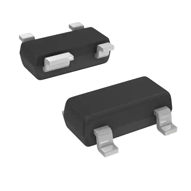
文档中提供了MSA-2111的引脚连接和封装标记图示。SOT-143封装的标记提供了方向和识别信息。

4. 参数特性: - 绝对最大额定值包括设备电流40mA、功率耗散125mW、射频输入功率+13dBm、结温150°C、存储温度-65°C至150°C。 - 电气特性包括功率增益(Gp)在900MHz时为16.0dB至17.5dB、增益平坦度(AGp)在0.1至0.3GHz时为±0.5dB、3dB带宽(f3dB)为0.5GHz、输入和输出电压驻波比(VSWR)在0.1至2.5GHz时为1.8:1、噪声系数(NF)在900MHz时为3.3dB、1dB增益压缩输出功率(P1dB)在900MHz时为10dBm、三阶截取点(IP3)在900MHz时为20dBm、群延迟(tD)在900MHz时为158psec、器件电压(Vd)在2.9V至4.3V之间变化、器件电压温度系数(dV/dT)为-8.0mV/°C。

5. 功能详解: - MSA-2111系列使用Avago的10GHz fT、25GHz fMAX硅双极MMIC工艺制造,该工艺使用氮化物自对准、离子注入和金金属化,以实现卓越的性能、均匀性和可靠性。使用外部偏置电阻以实现温度和电流稳定性,也允许偏置灵活性。

6. 应用信息: - 典型应用包括商业和工业应用中的窄带和宽带中频(IF)和射频(RF)放大器。

7. 封装信息: - MSA-2111采用表面贴装塑料SOT-143封装,提供胶带和卷轴包装选项,也有无铅选项可用。
MSA-2111-BLKG 价格&库存

很抱歉,暂时无法提供与“MSA-2111-BLKG”相匹配的价格&库存,您可以联系我们找货

免费人工找货