X5R Dielectric, KGM Series
General Specifications
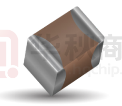
GENERAL DESCRIPTION
• General Purpose Dielectric for Ceramic Capacitors
• EIA Class II Dielectric
• Temperature variation of capacitance is within ±15%
from -55°C to +85°C
• Well suited for decoupling and filtering applications
• Available in High Capacitance values (up to 100μF)
HOW TO ORDER
KGM
03
A
R5
1E
101
M
N
Series
General Purpose
Tin/Nickel Finish
Size
02 = 01005
03 = 0201
05 = 0402
15 = 0603
21 = 0805
31 = 1206
32 = 1210
43 = 1812
Thickness
See Cap Chart
Dielectric
R5 = X5R
Voltage
0G = 4.0V
0J = 6.3V
1A = 10V
1C = 16V
1E = 25V
1H = 50V
Capacitance
Code Code (in pF)
Capacitance
Tolerance
Packaging
See Table Below
Two Significant Digits +
Number of zeroes
eg. 106 = 10uF
103 = 10nF
470 = 47pF
J* = +/- 5%
K = +/- 10%
M = +/- 20%
NOTE: Contact factory for availability of Tolerance Options for Specific Part Numbers.
Contact factory for non-specified capacitance values.
PACKAGING CODES
Code
EIA
(inch)
IEC(mm)
7"
Paper
7"
Embossed
13"
Paper
13"
Embossed
02
01005
0402
H
P
N
03
0201
0603
H
05
0402
1005
H
N
15
0603
1608
T
M
21
0805
2012
U
L
31
1206
3216
U
L
32
1210
3225
U
L
43
1812
4532
V
S
N
20
15
% Capacitance
10
0
-5
-10
-15
-20
-60
-40
-20
0
+20
+40
Temperature °C
+60
+80
Insulation Resistance (Ohm-Farads)
TYPICAL ELECTRICAL CHARACTERISTICS
10,000
Insulation Resistance vs Temperature
1,000
100
0
20
40
60
80
100
120
Temperature °C
The Important Information/Disclaimer is incorporated in the catalog where these specifications came from or available
online at www.kyocera-avx.com/disclaimer/ by reference and should be reviewed in full before placing any order.
TDS-SMDMLCC-0035 | Rev 2
– surface mount ceramic capacitor products –
1
�X5R Dielectric, KGM Series
Specifications and Test Methods
X5R Specification Limits
X5R Specification Limits
Operating Temperature Range
-55ºC to +85ºC
Capacitance
Within specified tolerance
Measuring Conditions (Complies with JIS C5101 / IEC60384)
Temperature Cycle Chamber
Measure after heat treatment
Capacitance Frequency Volt
C≤10µF
Frequency : 1kHz±10%
Volt : 1.0±0.2Vrms *0.5±0.2Vrms
* :KGM02AR50J104, KGM02AR50J474,
KGM03CR50J225, KGM03BR50J225
Dissipation Factor / Tanδ
Refer to https://spicat.kyocera-avx.com for individual part number specification
KGM03DR50J475, KGM03CR50G475,
KGM05CR50J106
C>10µF
Frequency : 120Hz±10%
Volt : 0.5±0.2Vrms
The charge and discharge current of the capacitor must not exceed 50mA.
Insulation Resistance
Refer to https://spicat.kyocera-avx.com for individual part number specifiction
Dielectric Strength
No breakdown or visual defects
Bending Strength
No significant damage with 1mm bending
Solderability
Solder coverage : 95% min.
Resistance to Solder
Heat
Appearance
No problem observed
Capacitance Variation
≤ ±7.5%
Dissipation Factor / Tanδ
Within specification
Insulation Resistance
Within specification
Apply the rated voltage for 1 minute, and measure it in normal temperature and humidity.
The charge and discharge current of the capacitor must not exceed 50mA.
Charge device with 250% of rated voltage for 1-5 seconds, w/ charge and discharge current limited to 50 mA (max)
* KGM31AR52A225: 200% of rated voltage
Glass epoxy PCB: Fulcrum spacing: 90mm, duration time 10 seconds.
Soaking condition
Sn-3Ag-0.5Cu 245±5℃ 3±0.5 sec.
Take the initial value after heat treatment.
Soak the sample in 260℃±5℃ solder for 10±0.5 seconds and place in nor- mal temperature and humidity, and measure after
heat treatment.
(Pre-heating conditions)
Order Temperature Time
1 80 to 100℃ 2 minutes
2
Withstanding Voltage / Dielectric
Resist without problem
Strength
150 to 200℃
2 minutes
The charge and discharge current of the capacitor must not exceed 50mA for IR and withstanding voltage measurement.
Appearance
No visual defects
Take the initial value after heat treatment.
Capacitance Variation
≤ ±7.5%
Room temperature (3 min.) ―>
Dissipation Factor
Within specification
Insulation Resistance
Within specification
(Cycle)
Thermal Shock
Withstanding Voltage / Dielectric
Room temperature (3 min.) ―>
Highest operation temperature (30 min.)
After 5 cycles, measure after heat treatment.
Resist without problem
Strength
Load Life
Lowest operation temperature (30 min.) ―>
Appearance
No visual defects
Capacitance Variation
≤ ±12.5%
The charge and discharge current of the capacitor must not exceed 50mA for IR and withstanding voltage measurement.
Take the initial value after heat treatment.
After applying *1.5 the rated voltage at the highest operation temperature for 1000+12/ −0 hours, and measure the sample
after heat treatment in normal temperature and humidity.
The charge and discharge current of the capacitor must not exceed 50mA for IR measurement.
Dissipation Factor / Tanδ
≤ Initial Value x 2.0 (See Above)
Over 1000MΩ or 50MΩ・µF, whichever is less. *Exceptions Listed Below
in the chart below.
Appearance
No visual defects
Take the initial value after heat treatment.
Capacitance Variation
Load Humidity
*Apply 1.0 times when the rated voltage is 4V or less. Applied voltages for respective products are indicated
Insulation Resistance
After applying rated voltage for 500+12/ −0 hours in the condition of 40℃±2℃ and 90 to 95%RH, and place in normal
≤ ±12.5%
Dissipation Factor / Tanδ
Within specification
temperature and humidity, then measure the sample after heat treatment.
Insulation Resistance
Over 1000MΩ or 50MΩ · µF, whichever is less. *Exceptions Listed Below
The charge and discharge current of the capacitor must not exceed 50mA for IR measurement.
Appearance
No problem observed
Microscope
Termination Strength
No problem observed
Apply a sideward force of 500g (5N) to a PCB-mounted sample. note : 2N for 0201 size, and 1N for 01005 size.
Appearance
No problem observed
Take the initial value after heat treatment.
Capacitance
Within tolerance
Vibration frequency: 10 to 55 (Hz)
Vibration
Tanδ
Heat treatment
Within tolerance
Amplitude: 1.5mm
Sweeping condition: 10 ―> 55 ―> 10Hz/ 1 minute in X, Y and Z directions: 2
hours each, 6 hours in total, and place in normal temperature and humidity, then measure the sample after heat treatment.
Expose sample in the temperature of 150+0/ −10℃ for 1 hour and leave the sample in normal temperature and humidity for 24±2 hours.
Voltage to be applied in the High Temperature Load (Applied voltage is the multiple of the rated voltage)
Rated Voltage
×1.0
×1.2
×1.3
Products
6.3V
KGM02AR50J224, KGM02AR50J474, KGM03BR50J225, KGM03CR50J225, KGM03DR50J475, KGM05CR50J106, KGM05BR50J156, KGM05DR50J226, KGM21AR50J476
10V
KGM02AR51A104, KGM03CR51A225, KGM15CR51A226
16V
KGM03CR51C105, KGM05AR51C225, KGM05CR51C475, KGM15CR51C226
25V
KGM05AR51E105, KGM05AR51E225, KGM05CR51E225, KGM05CR51E475, KGM15CR51E475, KGM15CR51E106, KGM21AR51E226
35V
KGM05AR51V105, KGM15CR51V475, KGM15CR51V106
100V
KGM31AR52A225
6.3V
KGM03BR50J105
6.3V
KGM02AR50J153-104, KGM03AR50J474
10V
KGM03AR51A223-224, KGM05AR51A105-225
16V
KGM05AR51C105
Insulation Resistance : Over 10MΩ・μF
X5R / R5
2
03
KGM03BR51A105, KGM03CR51C224, KGM03CR51E224
05
KGM05BR51A475, KGM05CR51A106, KGM05CR51V225
The Important Information/Disclaimer is incorporated in the catalog where these specifications came from or available
online at www.kyocera-avx.com/disclaimer/ by reference and should be reviewed in full before placing any order.
TDS-SMDMLCC-0035 | Rev 2
– surface mount ceramic capacitor products –
�X5R Dielectric, KGM Series
Capacitance Range
Case Size
01005
0201
0402
0603
0805
Soldering
Reflow Only
Reflow Only
Reflow/Wave
Reflow/Wave
Reflow/Wave
Packaging
mm
(in.)
mm
(in.)
mm
(in.)
(L) Length
W) Width
(t) Terminal
Voltage:
Cap (pF)
Cap (μF)
100
Paper/Embossed
All Paper
All Paper
All Paper
All Embossed
0.40 ± 0.02
(0.016 ± 0.0008)
0.20 ± 0.02
(0.008 ± 0.0008)
0.10 ± 0.04
(0.004 ± 0.0016)
0.60 ± 0.09
(0.024 ± 0.004)
0.30 ± 0.09
(0.011 ± 0.004)
0.15 ± 0.05
(0.006 ± 0.002)
1.00 ± 0.20
(0.040 ± 0.008)
0.50 ± 0.20
(0.020 ± 0.008)
0.25 ± 0.10
(0.010 ± 0.004)
1.60 ± 0.20
(0.063 ± 0.008)
0.80 ± 0.20
(0.031 ± 0.008)
0.35 ± 0.15
(0.014 ± 0.006)
2.01 ± 0.20
(0.079 ± 0.008)
1.25 ± 0.20
(0.049 ± 0.008)
0.50 ± 0.25
(0.020 ± 0.010)
6.3
101
10
16
A
A
4
6.3
10
16
25
4
6.3
10
16
25
35
50
150
151
A
A
A
220
221
A
A
A
A
330
331
A
A
A
A
470
471
A
A
A
A
680
681
A
A
A
A
1000
102
1500
152
A
4
6.3
10
16
25
35
50
A
A
A
A
A
A
A
A
A
A
2200
222
A
A
A
A
A
A
A
3300
332
A
A
A
A
A
A
A
4700
472
A
A
A
A
A
A
A
A
6800
682
A
A
A
A
A
A
A
A
A
A
A
A
A
0.010
103
A
0.015
153
A
0.022
223
A
0.033
333
A
0.047
473
A
0.068
683
A
0.10
104
A
0.15
154
0.22
224
0.33
334
0.47
474
0.68
684
A
A
A
A
A
A
A
A
A
A
10
16
A
A
35
50
A
A
A
A
A
A
A
A
A
A
A
A
A
A
K
A
A
A
K
A
A
K
K
K
B
B
K
K
A
A
A
B
A
A
C
C
A
A
A
A
A
A
A
A
A
K
A
A
K
A
A
25
A
A
A
A
A
A
A
1
105
B
B
B/C
225
C
B/C
C
4.7
475
C
D
10
106
C
A
A
H
A
H
B
B
B
B
B
B
B
B
B
B
B
B
B
B
B
B
B
B
B
B
B
B
A
A
A
A
A
A
B
B
B
B
B
B
B
A
A
A
A/C
C
B
B
B
B
B
C
C
H
H
B/C
C
C
C
C
C
15
156
B
B
226
C
D
47
476
100
107
A
A
A
A
A
A
A
A
A
A
A
A
A
A
A
35
50
B
B
B
C
C
A
A
A
A
A
C
C
C
C
C
A
A
A
A
A
C
C
A
A
16
25
C
C
4
6.3
K
A
B
C
K
A
C
C
K
A
A
22
Case Size
6.3
A
A
A
A
2.2
Voltage:
4
A
A
A
A
A
A
A
4
6.3
A
6.3
10
16
4
6.3
01005
Case Size
01005 (KGM 02)
Thickness Letter
Max Thickness (mm)
Carrier Tape
Packaging Code 7"reel
Packaging Code 13"reel
A
0.22
PAPER
H
P
10
16
25
4
6.3
0201
10
16
25
35
0402
H
N
B
C
0.35
0.39
PAPER
H
H
N
N
10
16
25
35
50
10
0603
0201 (KGM03)
A
0.33
50
0805
0402 (KGM05)
D
0.55
A
0.55
B
0.65
H
N
H
N
H
N
C
0.70
PAPER
H
N
0603 (KGM15)
H
0.75
D
0.8
A
0.90
H
N
H
N
T
M
PAPER
B
C
0.95
1
PAPER
T
T
M
M
– surface mount ceramic capacitor products –
K
1.40
T
M
U
L
A
1.45
EMB
U
L
EMBOSSED (EMB)
The Important Information/Disclaimer is incorporated in the catalog where these specifications came from or available
online at www.kyocera-avx.com/disclaimer/ by reference and should be reviewed in full before placing any order.
TDS-SMDMLCC-0035 | Rev 2
0805 (KGM21)
D
1.02
3
�X5R Dielectric, KGM Series
Capacitance Range
PREFERRED SIZES ARE SHADED
Case Size
1206
1210
1812
Soldering
Reflow/Wave
Reflow Only
Reflow Only
All Embossed
All Embossed
All Embossed
3.20 ± 0.40
(0.126 ± 0.016)
1.60 ± 0.30
(0.063 ± 0.012)
0.50 ± 0.25
(0.020 ± 0.010)
3.20 ± 0.40
(0.126 ± 0.016)
2.50 ± 0.30
(0.098 ± 0.012)
0.50 ± 0.25
(0.020 ± 0.010)
4.50 ± 0.30
(0.177 ± 0.012)
3.20 ± 0.20
(0.126 ± 0.008)
0.61 ± 0.36
(0.024 ± 0.014)
Packaging
mm
(in.)
mm
(in.)
mm
(in.)
(L) Length
W) Width
(t) Terminal
Voltage:
Cap (pF)
Cap (μF)
100
101
150
151.0
220
221
330
331
470
471
680
681
1000
102
1500
152
2200
222
3300
332
3900
392
4700
472
5600
562
6800
682
0.01
103
0.012
123
0.015
153
0.018
183
0.022
223
0.027
273
0.033
333
0.039
393
0.047
473
0.068
683
0.082
823
0.10
104
0.12
124
0.15
154
0.22
224
0.33
334
0.47
474
0.68
684
4
6.3
10
16
25
35
50
M
M
M
M
M
M
M
1
105
H
H
H
H
H
H
H
2.2
225
H
H
H
H
H
H
H
4.7
475
H
H
H
H
H
H
A
10
106
H
H
H
H
A
H
H
22
226
H
H
H
A
H
H
H
47
476
H
H
100
107
H
H
4
6.3
Voltage:
10
16
Case Size
35
A
50
100
4
6.3
10
A
1.8
EMB
U
L
C
1.27
EMB
U
L
35
50
C
C
E
E
E
E
E
E
L
L
L
L
L
L
L
J
J
J
J
J
A
A
A
A
J
J
J
J
J
A
A
A
A
A
L
L
L
16
25
L
L
L
L
4
6.3
1210 (KGM 32)
H
1.9
EMB
U
L
25
10
35
50
4
6.3
10
J
J
J
4
6.3
10
E
1.45
EMB
U
L
J
2.21
EMB
U
L
1812 (KGM 43)
A
2.7
EMB
U
L
L
2.80
EMB
U
L
J
2.80
EMB
V
S
EMBOSSED (EMB)
4
The Important Information/Disclaimer is incorporated in the catalog where these specifications came from or available
online at www.kyocera-avx.com/disclaimer/ by reference and should be reviewed in full before placing any order.
TDS-SMDMLCC-0035 | Rev 2
– surface mount ceramic capacitor products –
16
25
35
50
35
50
J
1210
1206 (KGM 31)
M
1.25
EMB
U
L
16
E
1206
Case Size
Thickness Letter
Max Thickness (mm)
Carrier Tape
Packaging Code 7"reel
Packaging Code 13"reel
25
100
16
1812
25
��


 工商网监
湘ICP备2023018690号
工商网监
湘ICP备2023018690号
