F91 Series
Low ESR, Resin-Molded Chip J-Lead
FEATURES
• Compliant to the RoHS2 directive 2011/65/EU
• SMD J-lead
• Low ESR
LEAD-FREE COMPATIBLE
COMPONENT
APPLICATIONS
• General medium power DC/DC convertors
CASE DIMENSIONS: millimeters (inches)
1210
3528-21
C
2312
6032-27
N
2917
7343-30
L
3.50 ± 0.20
(0.126 ± 0.008)
6.00 ± 0.20
(0.236 ± 0.008)
7.30 ± 0.20
(0.287 ± 0.008)
B CASE
W1
2.80 ± 0.20
(0.110 ± 0.008)
3.20 ± 0.20
(0.126 ± 0.008)
4.30 ± 0.20
(0.169 ± 0.008)
W2
2.20 ± 0.10
(0.087 ± 0.004)
2.20 ± 0.10
(0.087 ± 0.004)
2.40 ± 0.10
(0.094 ± 0.004)
C, N CASE
L
B CASE
W1
Capacitance
(µF)
22
16V
W2
HOW TO ORDER
F91
1A
107
Rated
Voltage
Capacitance
Code
pF code: 1st two digits
represent significant figures,
3rd digit represents multiplier
(number of zeros to follow)
C CASE
Capacitance
(µF)
N CASE
Capacitance
(µF)
S
Rated Voltage
(V)
Type
S
0.80 ± 0.20
(0.031 ± 0.008)
1.30 ± 0.20
(0.051 ± 0.008)
1.30 ± 0.20
(0.051 ± 0.008)
MARKING
H
S
H
1.90 ± 0.20
(0.075 ± 0.008)
2.50 ± 0.20
(0.098 ± 0.008)
2.80 ± 0.20
(0.110 ±0.008)
220
10V
B
68
10V
Code EIA Code EIA Metric
M
C
ⵧ
Tolerance
K = ±10%
M = ±20%
Case
Size
See
table
above
Packaging
See Tape & Reel
Packaging Section
Rated Voltage
(V)
Rated Voltage
(V)
TECHNICAL SPECIFICATIONS
Category Temperature Range:
Rated Temperature:
Capacitance Tolerance:
Dissipation Factor:
ESR 100kHz:
Leakage Current:
Capacitance Change By Temperature
86
-55 to +125°C
+85°C
±20%, ±10% at 120Hz
Refer to next page
Refer to next page
After 1 minute’s application of rated voltage, leakage current at 20°C
is not more than 0.01CV or 0.5μA, whichever is greater.
After 1 minute’s application of rated voltage, leakage current at 85°C
is not more than 0.1CV or 5μA, whichever is greater.
After 1 minute’s application of derated voltage, leakage current at 125°C
is not more than 0.125CV or 6.3μA, whichever is greater.
+15% Max. at +125°C
+10% Max. at +85°C
-10% Max. at -55°C
051718
�F91 Series
Low ESR, Resin-Molded Chip J-Lead
CAPACITANCE AND RATED VOLTAGE RANGE (LETTER DENOTES CASE SIZE)
Capacitance
µF
Code
6.8
685
10
106
15
156
22
226
33
336
47
476
68
686
100
107
150
157
220
227
330
337
470
477
680
687
Rated Voltage
6.3V (0J)
10V (1A)
4V (0G)
16V (1C)
20V (1D)
25V (1E)
C
C
B
C
C
N
N
N
C
C
C/N
N
N
C
C
N
N
N
B
B/C
N
N
N
N
N
N
35V (1V)
C
N
N
N
N
Released ratings
RATINGS & PART NUMBER REFERENCE
AVX
Part No.
Case
Size
Capacitance
(μF)
Rated
Voltage
(V)
F910G157#CC
F910G227#CC
F910G337#NC
F910G477#NC
F910G687#NC
C
C
N
N
N
150
220
330
470
680
4
4
4
4
4
F910J107#CC
F910J157#CC
F910J227#CC
F910J227#NC
F910J337#NC
F910J477#NC
C
C
C
N
N
N
100
150
220
220
330
470
6.3
6.3
6.3
6.3
6.3
6.3
F911A476#BA
F911A686#CC
F911A107#CC
F911A157#NC
F911A227#NC
F911A337#NC
B
C
C
N
N
N
47
68
100
150
220
330
10
10
10
10
10
10
F911C226#BA
F911C336#BA
F911C336#CC
F911C476#NC
F911C107#NC
B
B
C
N
N
22
33
33
47
100
16
16
16
16
16
F911D156#CC
F911D336#NC
F911D476#NC
C
N
N
15
33
47
20
20
20
F911E106#CC
F911E226#NC
F911E336#NC
F911E476#NC
C
N
N
N
10
22
33
47
25
25
25
25
F911V685#CC
F911V106#NC
F911V156#NC
F911V226#NC
C
N
N
N
6.8
10
15
22
35
35
35
35
DCL
(μA)
4 Volt
6.0
8.8
13.2
18.8
27.2
6.3 Volt
6.3
9.5
13.9
13.9
20.8
29.6
10 Volt
4.7
6.8
10.0
15.0
22.0
33.0
16 Volt
3.5
5.3
5.3
7.6
16
20 Volt
3
6.6
9.4
25 Volt
2.5
5.5
8.3
11.8
35 Volt
2.4
3.5
5.3
7.7
DF
@ 120Hz
(%)
ESR
@ 100kHz
(mΩ)
100kHz RMS Current
(mA)
20ºC
MSL
12
12
10
16
18
250
250
100
100
100
663
663
1225
1225
1225
1
1
1
1
1
8
12
14
10
14
16
250
250
250
100
100
100
663
663
663
1225
1225
1225
1
1
1
1
1
1
8
8
10
10
12
18
500
300
250
100
100
100
412
606
663
1225
1225
1225
1
1
1
1
3
3
8
8
6
6
10
950
950
400
150
100
299
299
524
1000
1225
1
1
1
1
3
6
6
8
450
200
200
494
866
866
1
1
1
6
6
8
8
450
200
200
250
494
866
866
775
1
1
1
1
6
6
6
8
600
300
300
300
428
707
707
707
1
1
1
1
#: "M" for ±20% tolerance, "K" for ± 10% tolerance.
Moisture Sensitivity Level (MSL) is defined according to J-STD-020.
051718
87
�F91 Series
Low ESR, Resin-Molded Chip J-Lead
QUALIFICATION TABLE
TEST
Damp Heat
(Steady State)
Temperature Cycles
Resistance to
Soldering Heat
Surge
Endurance
Shear Test
Terminal Strength
88
F91 series (Temperature range -55ºC to +125ºC)
Condition
At 40°C, 90 to 95% R.H., 500 hours (No voltage applied)
Capacitance Change ........... Within ±10% of the initial value
Dissipation Factor ................ Initial specified value or less
Leakage Current .................. Initial specified value or less
-55°C / +125°C, 30 minutes each, 5 cycles
Capacitance Change ........... Within ±5% of the initial value
Dissipation Factor ................ Initial specified value or less
Leakage Current .................. Initial specified value or less
10 seconds reflow at 260°C, 5 seconds immersion at 260°C.
Capacitance Change ........... Within ±5% of the initial value
Dissipation Factor ................ Initial specified value or less
Leakage Current .................. Initial specified value or less
After application of surge voltage in series with a 33Ω resistor at the rate of 30 seconds ON, 30 seconds OFF,
for 1000 successive test cycles at 85ºC, capacitors shall meet the characteristic requirements in the table above.
Capacitance Change ........... Within ±5% of the initial value
Dissipation Factor ................ Initial specified value or less
Leakage Current .................. Initial specified value or less
After 2000 hours’ application of rated voltage in series with a 3Ω resistor at 85°C, or derated voltage in series with a 3Ω
resistor at 125°C, capacitors shall meet the characteristic requirements in the table above.
Capacitance Change ........... Within ±10% of the initial value
Dissipation Factor ................ Initial specified value or less
Leakage Current .................. Initial specified value or less
After applying the pressure load of 5N for 10±1 seconds horizontally to the center of capacitor side body
which has no electrode and has been soldered beforehand on a substrate, there shall be found neither
exfoliation nor its sign at the terminal electrode.
Keeping a capacitor surface-mounted on a substrate upside down and supporting the substrate at
both of the opposite bottom points 45mm apart from the center of capacitor, the pressure strength is
applied with a specified jig at the center of substrate so that the substrate may bend by 1mm as illustrated. Then, there shall be found no remarkable abnormality on the capacitor terminals.
051718
�F91 Series
Low ESR, Resin-Molded Chip J-Lead
AVX SOLID ELECTROLYTIC CAPACITOR ROADMAP
SERIES LINE UP: CONVENTIONAL SMD MnO2
051718
89
�
很抱歉,暂时无法提供与“F911E336MNC”相匹配的价格&库存,您可以联系我们找货
免费人工找货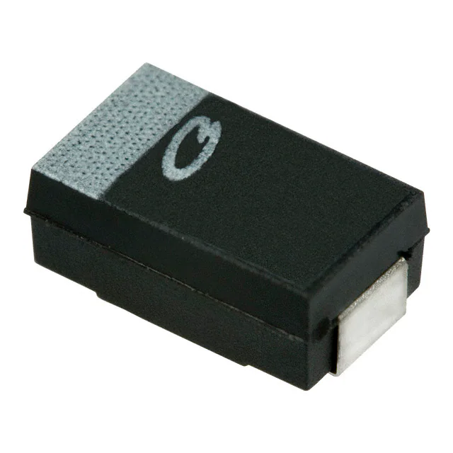


 工商网监
湘ICP备2023018690号
工商网监
湘ICP备2023018690号
