KC2016K64.0000C3GN00 数据手册
Specification
Drawing No.
TNY1T-H1-SEN01-00 [1/7]
Issued Date.
1-Oct-18
TO: Digikey
Note:In case of specification change, KYOCERA Part Number also will be changed.
Product Name
Crystal Oscillator
Product Model
Frequency
Customer Part Number
Customer Specification Number
64 MHz
--
KYOCERA Part Number KC2016K64.0000C3GN00
Remarks RoHS Compliant / MSL 1
Customer Acceptance
Accept Signature
Accept Date
Department
Person in charge
KYOCERA Corporation
Head Office
Sales Division
6 Takeda Tobadono-cho, Fushimi-ku, Kyoto
612-8501 Japan
TEL. No. (+81)75-604-3500
FAX. No. (+81)75-604-3501
6 Takeda Tobadono-cho, Fushimi-ku, Kyoto
612-8501 Japan
TEL. No. (+81)75-604-3500
FAX. No. (+81)75-604-3501
Design Department
KYOCERA Corporation
Crystal Components Division
Quality
Assurance
Approved by Checked by
Issued by
�Drawing No.
TNY1T-H1-SEN01-00 [2/7]
Revision History
Description of revise
Rev. No.
00
First Edition
Date
1-Oct-18
KYOCERA Corporation
Approved by Checked by Issued by
�Drawing No.
TNY1T-H1-SEN01-00 [3/7]
1. Scope
This specification shall be defined of the Clock Oscillator for the integrated circuits (ICs).
2. Customer Part Number
--3. KYOCERA Part Number
KC2016K64.0000C3GN00
4. Electrical Characteristics
4-1. Absolute Maximum Rating
Item
Power Supply Voltage
Units
V
VIN
Rated Value
-0.3 to +7.0
-0.3 to VCC +0.3
TSTG
-55 to +125
°C
Symbol
VCC
Input Voltage
Storage Temperature
V
Note:
If the part is used beyond absolute maximum ratings, it may cause internal destruction. The part should be used under the recommended operating conditions
the reliability of this part may be damaged if those conditions are exceeded.
4-2. Recommended Operating Conditions
Item
Symbol
VCC
Power Supply Voltage
Units
V
---
-40
25
+85
°C
Symbol
FO
Min
--
Typ
64
Max
--
Units
MHz
Frequency Tolerance*
F_tol
-50
--
+50
ppm
Current Consumption
ICC
--
--
18
mA
Standby Current
IST
--
--
10
µA
SYM
45
50
55
%
Tr/ Tf
--
--
5
ns
VOL
--90% VCC
---
10% VCC
V
IOL= 8mA
---
---
V
IOH= -8mA
---
---
pF
Operating Temperature
4-3. Electrical Characteristics
Item
Output Frequency
Symmetry (Duty Ratio)
Rise Time/ Fall Time
(10% VCC to 90% VCC)
Output Voltage-“L”
Typ
3.3
VIN
0
TOPR
Remarks
Max
3.63
VCC
Input Voltage
Min
2.97
V
Output Voltage-“H”
VOH
Output Load
Input Voltage-“L”
CL
VIL
---
Input Voltage-“H”
VIH
--70% VCC
15
30% VCC
---
---
V
Output Disable Time
t_dis
---
---
150
ns
Output Enable Time
t_ena
---
---
5
ms
Start-up Time
t_sta
---
---
5
ms
1 Sigma Jitter**
JSigma
---
---
4
ps
Peak to Peak Jitter**
JPK-PK
---
---
40
ps
---
-----------------
---92
-126
-151
-160
-167
-170
-170
0.5
---------------
ps
Phase Jitter
Phase Noise
@25MHz Typical
---
Remarks
@50% Vcc
CMOS
V
@Minimum operating
voltage to be 0sec
BW:12kHz to 20MHz
@10Hz offset
@100Hz offset
@1kHz offset
dBc/Hz
@10kHz offset
@100kHz offset
@1MHz offset
@10MHz offset
Note: All electrical characteristics have defined on the maximum loaded and recommended operating conditions.
* Include initial tolerance, operating temperature range, rated power supply voltage change, load change,
aging (1year @+25°C), shock and vibration
**Based on Time Interval Analyzer "Wavecrest SIA-3000”.
Table 1
KYOCERA Corporation
�Drawing No.
TNY1T-H1-SEN01-00 [4/7]
4-4. Measurement Condition
The reference temperature shall be +25±2ºC. The measurement shall be performed at the
temperature range of +5 ºC to +35 ºC unless otherwise the result is doubtful.
4-5. Measurement Circuit
The electrical characteristics shall be measured by test circuit "Fig. 1". Also jitter shall be
measured by test circuit "Fig. 3".
4-6. Clock Timing Chart
Tr
Tf
The clock timing chart is "Fig. 2".
Test Point
Pad4
VCC
Pad3
VOH
A
90%VCC
Oscillator
+
Pad1
Power
Supply
50%VCC
Pad2
V
CL
0.01µF
10%VCC
VOL
-
E/D Control
GND
T1
Note: CL includes probe and test fixture capacitance
Fig.1 Test Circuits
Clock Oscillator Test Fixture
Pad4
Fig.2 Clock Timing Chart (C-MOS Output)
50 ohm SMA Termination
Pad3
WaveCrest
SIA-3000
Pad2
ATT 6dB
Oscillator
+
Pad1
Power
Supply
10µF 0.01µF
-
E/D Control
Symmetry = T1/ T0 X100(%)
T0 = 1/fOUT
50 ohm COAX with SMA Connectors
l Time Interval Analyzer
WaveCrest SIA-3000
l DTS timer calibration
Over 30 minutes warm-up
Extend 30 minutes calibration
l Jitter histogram conditions (Tail-fit)
More than 50,000cyc Hits
Bit Error Ratio (BER) –12 (14sigma)
Fig.3 Jitter Test Circuits
5. Dimensions and Marking
1.2
0.4
#3
#4
Pad1 Indication
□ P4A
0.6
#1
Manufacturing Date Code
Output Frequency
The output frequency is three-digit without a decimal
point. The frequency greater than the number of
digits have rounded down.
0.8 Max
#2
0.24
(E.g. 14.31818MHz "14N3”)
Plating Ni+Au
Tolerance:+/-0.2 Manufacturing Date Code
Unit:(mm)
Pad arrangement
1
2
3
4
64N0
0.4
1.6
Marking Area
Output Frequency
0.6
0.4
2.0
Enable/Disable
Case GND
Output
VCC
Enable/Disable Function
Pad1
OPEN
“H” Level
Pad3 (Output)
Active
Active
“L” Level
High Z (No-Oscillation)
Year
Code
Year
Code
Month
Code
2001
2002
A
B
2011
2012
L
M
1
2
1
2
1
2
1
2
11
12
B
C
21
22
M
N
2003
2004
2005
2006
2007
2008
2009
2010
C
D
E
F
G
H
J
K
2013
2014
2015
2016
2017
2018
2019
2020
N
P
Q
R
S
T
V
W
3
4
5
6
7
8
9
10
11
12
3
4
5
6
7
8
9
A
B
C
3
4
5
6
7
8
9
10
3
4
5
6
7
8
9
A
13
14
15
16
17
18
19
20
D
E
F
G
H
J
K
L
23
24
25
26
27
28
29
30
31
P
Q
R
S
T
V
W
X
Y
It repeats from A in 2021 and
afterw ards.
Day Code
Day Code
e.g. :”P4A” means “Apr-10-2014”
Table 2
KYOCERA Corporation
Day Code
�Drawing No.
TNY1T-H1-SEN01-00 [5/7]
6. Parts Numbering Guide
KC2016K 64.0000 C 3 G N 00
A
B
A. Series (SMD Oscillator)
B. Output Frequency
C. Output
C: C-MOS
D. Supply Voltage
3: 3.3V
E. Frequency Tolerance*
G: ±50ppm
7-2. Soldering Heat
Resistance
7-3. Temperature Cycle
7-4. Mechanical
Shock (Pulse)
7-5. Vibration
7-6. High Temperature
7-7. Low Temperature
7-8. Humidity Cycle
7-9. Hermeticity 1
(Gross leak)
7-10.Hermeticity 2
(Fine leak)
G
F: Symmetry (Duty Ratio) and Enable/Disable Function
N: Symmetry: 45% to 55% with Stand-by Function
G. Suffix for Individual Requirements
(STD Specification is ''00'')
Packing (Tape & Reel 2,000pcs/Reel)
*Over All Conditions:
Include initial tolerance, operating temperature range,
rated power supply voltage change, load change,
aging (1year @+25°C), shock and vibration
7. Environmental Characteristics
Items
7-1. Solderability
C D E F
Conditions
Soaking:
+245±5°C, 5.0±0.5sec
Reflow soldering:
Peak +260°C max, 10sec, Twice max
10cycles:
-55°C to +125°C (30minuts each/ cycle)
5 times
14,750m/sec2 (1,500G), Duration of pulse 0.5msec
(MIL-STD-883D-2002.3 Condition B)
4 times each axis X, Y, Z:
20 to 2,000Hz and 2,000Hz to 20Hz/cycle
Peak acceleration 196m/sec2 (20G)
(MIL-STD-883D-2007.2 Condition A)
1000 hours:
Temperature: +85+5/-3°C
1000 hours:
Temperature: -40+5/-3°C
10 cycles:
Based on 1004 specifications
(MIL-STD-883D-1004.7)
Soaking:
+125°C, 5minutes
Measured by Helium Detector Equipment
(MIL-STD-883D-1014.10 Condition A1)
Criteria of Acceptance
Dipped potion:
Minimum 95% coverage
Without looseness or crack etc
Clause 7-10 shall be satisfied.
Clause 7-1 shall be satisfied.
No bubbles appeared
5x10⁻⁹ Pa m3/sec max
After each testing, the parts shall be subjected to standard atmospheric conditions more than 2 hours. After that, the electrical
characteristics shall be measured. The result of the test shall be satisfied Table 1.
Table 3
KYOCERA Corporation
�Drawing No.
TNY1T-H1-SEN01-00 [6/7]
300
0.4
0.8
8. Recommended Land pattern and Soldering Guide
Temperature (ºC)
0.8
1.2
+255±5 ºC
+230 ºC
250
200
0.6
Unit: (mm)
+150 to +180 ºC
150
100
50
0.6
10sec max
Peak +260 ºC max
90 to 120 sec
0
30 to 40sec
Time (sec)
Available Reflow times: Maximum twice
Note:
Since the part doesn’t have Bypass Capacitor between V cc and
GND, Please mount high frequency type capacitor 0.01μF to the
nearest position of oscillator.
Fig.4 Land pattern
Fig.5 Reflow profile (Lead Free Available)
9. Taping Specifications
D0
T
P0
P2
E
K
W1
E
P1
A
W
B0
33.0
□ P4A
A0
N
F
D
C
D1
W2
Unit: (mm)
Symbol
Dimensions
Symbol
Dimensions
Symbol
Dimensions
A0
B0
W
F
E
1.8±0.1
2.25±0.1
8.0±0.2
3.5±0.05
1.75±0.1
P1
P2
P0
D0
T
4.0±0.1
2.0±0.05
4.0±0.1
1.5+0.1/-0
0.2±0.05
K
D1
0.9±0.1
1.1±0.1
Unit: (mm)
Symbol
Dimensions
Symbol
Dimensions
Symbol
Dimensions
Fig.6 Emboss Carrier Tape
A
N
W1
180 +0/-1.5
60+1/–0
9.0+0.3/-0
W2
C
D
11.4±1.0
13.0±0.2
21.0±0.8
E
2.0±0.5
Fig.7 Reel
9-1. Taping Quantities
• The taping of per reel shall be packed 2,000 pcs.
• The parts shall be contained continuously in the pocket.
9-2. Leader and Blank Pockets
• The package shall be consisted of leader, blank pockets and loaded pocket as follows “Fig. 8”.
• The power of peeling strength between top tape and carrier tape shall be 0.1N(10gf) to 0.7N(70gf) as
follows “Fig. 9”.
Top Tape
A) Leader
B) Blank Pocket (40mm to 320mm)
A+B: 400mm to 560mm
C) Load Pocket
D)
Carrier Tape
165º to 180º
Pulling Direction
Blank Pocket (160mm minimum)
Fig.8 Packing Method
Fig.9 Peeling Strength
KYOCERA Corporation
�Drawing No.
TNY1T-H1-SEN01-00 [7/7]
9-3. Reel Label
The reel label shall be consisted as below. (Based on EIAJ C-3 format)
A) Customer Part Number
D) Shipping Date
B) Lot No.
E) Vender Name
C) Quantities
9-4. Exterior Package Label
The oscillator shall be packed properly to avoid defect in transportation. The exterior package label shall be
consisted as below.
A) Name of Customer
E) Quantities
B) P/O No.
F) Shipping Date
C) Customer Part Number
G) Vender Name
D) Lot No.
10. The agreement of this specifications
In case there is any obscure point or doubt concerning the contents of the specification, it shall be settled
through consultation of both parties.
11. Remarks on Usages
A) Storage Conditions
The parts shall be stored in temperature range of -5 to +40 ° C, humidity 40 to 60% RH, and avoid direct
sunlight. Then the parts shall be used within 6 months.
B) Handling Conditions
Although the part has protection circuit against static electricity, when excess static electricity is applied, the
inside IC may get damaged.
Before mounting on the PCB, please make sure the direction of the part is correct. Otherwise the part of
temperature will increase. And also the part will have some damages.
Please do not use the parts under the unfavorable condition such as beyond specified range in this
specification.
Please do not use the parts under the condition, in the water or in the salt water also environment of dew or
harmful gas.
Please make sure the condition of pick and place following pick up nozzle guideline.
C)
D)
E)
F)
Picking Method:
Case of Head Unit 1.6 x 1.2mm (Inside Diameter)
The proper condition of pick and place will be different each equipment. Therefore, please check before
testing.
Rework Condition
Please do not pick up Head Unit. We can’t guaranty electrical performance and reliability.
Soldering Conditions
This product can respond to the general Pb-free reflow profile. The wave soldering cannot be supported.
Soldering in Mounting
In case of Solder paste and conductive glue contact product lid or product side face exception for product
terminal it’s possible to influence product characteristics.
Please be careful above contents.
Washing Conditions
Ultra sonic cleaning is available. However there is a possibility that Crystal in the part may cause damaged
under certain condition. Therefore please test before using.
After washing, please dry the parts completely. Otherwise water drops between the parts and PCB may
cause migration.
In case of using this part without above precaution, Kyocera is unable to guarantee the specific
characteristics.
KYOCERA Corporation
�
KC2016K64.0000C3GN00 价格&库存
很抱歉,暂时无法提供与“KC2016K64.0000C3GN00”相匹配的价格&库存,您可以联系我们找货
免费人工找货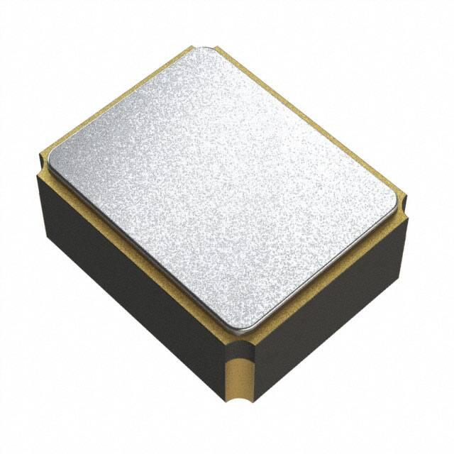


 工商网监
湘ICP备2023018690号
工商网监
湘ICP备2023018690号
