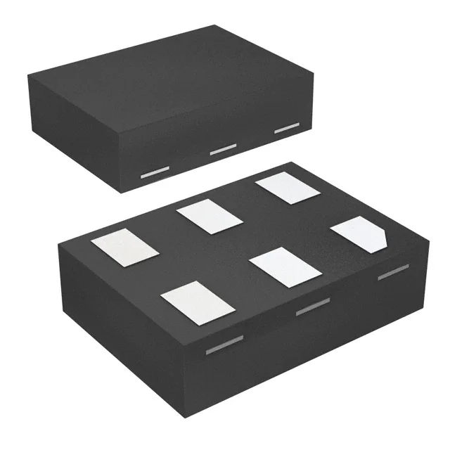
74AVC1T45
SINGLE BIT DUAL POWER SUPPLY TRANSLATING
TRANSCEIVER WITH 3 STATE OUTPUTS
Description
Pin Assignments
The 74AVC1T45 is a single bit, dual supply transceiver with tri-state
outputs suitable for transmitting a single logic bit across different
voltage domains. The A input/output pin is designed to track VCCA
while the B input/output tracks VCCB. This arrangement allows for
(Top View )
Vcc(A) 1
universal low-voltage translation between any voltages from 1.2V to
3.6V. The Direction pin (DIR) controls the direction of the transceiver
and in a logic voltage related to VCCA. When a high logic level is
6 Vcc(B)
GND 2
5 DIR
A 3
applied to DIR the A pin becomes an input and the B pin becomes the
output. Conversely the roles of A and B are reversed when DIR is
asserted low.
4 B
SOT26
SOT363
(Top View )
Vcc(A) 1
GND 2
A
(Bottom View)
The tri-state feature occurs when either of the power supply voltages
are zero. This is also an Ioff feature and allows for the output to
remain in a high-impedance state with both power supplies at 0V
preventing damaging backflow currents and providing power down
electrical isolation up to 3.6 V as not to interfere with any logic activity
on pin A or B.
A 3
GND 2
Vcc(A) 1
4B
5 DIR
3
6
Vcc(B)
5 DIR
4 B
X1-DFN1010-6
X2-DFN0910-6
X2-DFN1410-6
6 Vcc(B)
X2-DFN1409-6
Chip Scale
Alternative
Features
Applications
•
Wide Supply Voltage Range:
VCC(A): from 1.2V to 3.6V
VCC(B): from 1.2V to 3.6V
•
•
•
•
•
± 12mA Output Drive at 3.3V
High Noise Immunity—(100mV Hysteresis Typical)
IOFF Supports Partial-Power-Down Mode Operation
IOFF Controlled by Either VCC at 0V
•
•
Inputs Accept up to 4.6V
ESD Protection Exceeds JESD 22
200-V Machine Model (A115)
2000-V Human Body Model (A114)
1000 V Charged Device Model ( C101)
Latch-Up Exceeds 100mA per JESD 78, Class I
X2-DFN1409-6 Package Designed as a Direct Replacement for
Chip-Scale Packaging.
Totally Lead-Free & Fully RoHS Compliant (Notes 1 & 2)
Halogen and Antimony Free. “Green” Device (Note 3)
•
•
•
•
Notes:
•
•
Voltage Level Translation
Well Suited to Join Logic Types Operating at Different Voltages
Power Down Signal Isolation
If Either Voltage Domain is Turned off the Signal is Isolated and
There is no Loading on Signal Lines
Wide Array of Products, such as:
Cell Phones, Tablets, E-Readers
PCs, Notebooks, Netbooks, Ultrabooks
Networking, Routers, Gateways
Computer Peripherals, Hard Drives, CD/DVD ROMs
TVs, DVDs, DVRs, Set Top Boxes
Personal Navigation/GPS
MP3 players, Cameras, Video Recorders
1. No purposely added lead. Fully EU Directive 2002/95/EC (RoHS), 2011/65/EU (RoHS 2) & 2015/863/EU (RoHS 3) compliant.
2. See https://www.diodes.com/quality/lead-free/ for more information about Diodes Incorporated’s definitions of Halogen- and Antimony-free, "Green" and
Lead-free.
3. Halogen- and Antimony-free "Green” products are defined as those which contain
很抱歉,暂时无法提供与“74AVC1T45FZ4-7”相匹配的价格&库存,您可以联系我们找货
免费人工找货- 国内价格 香港价格
- 5000+0.925015000+0.11865
- 国内价格
- 1+0.72380
- 100+0.48202
- 1250+0.40194
- 2500+0.35574
- 5000+0.32340
