Preliminary Datasheet
LOW-POWER OFF-LINE PRIMARY SIDE REGULATION CONTROLLER
General Description
Features
The AP1680 is a high performance AC/DC power supply controller for LED drivers, battery charger and
adapter applications. The device uses Pulse Frequency
Modulation (PFM) method to build discontinuous conduction mode (DCM) flyback power supplies.
·
·
·
·
·
The AP1680 provides accurate constant voltage, constant current (CV/CC) regulation while removing the
opto-coupler and secondary control circuitry. It also
eliminates the need of loop compensation circuitry
while maintaining stability. The AP1680 achieves
excellent regulation and high average efficiency, yet
meets the requirement for no-load consumption less
than 30mW.
·
·
·
·
·
·
·
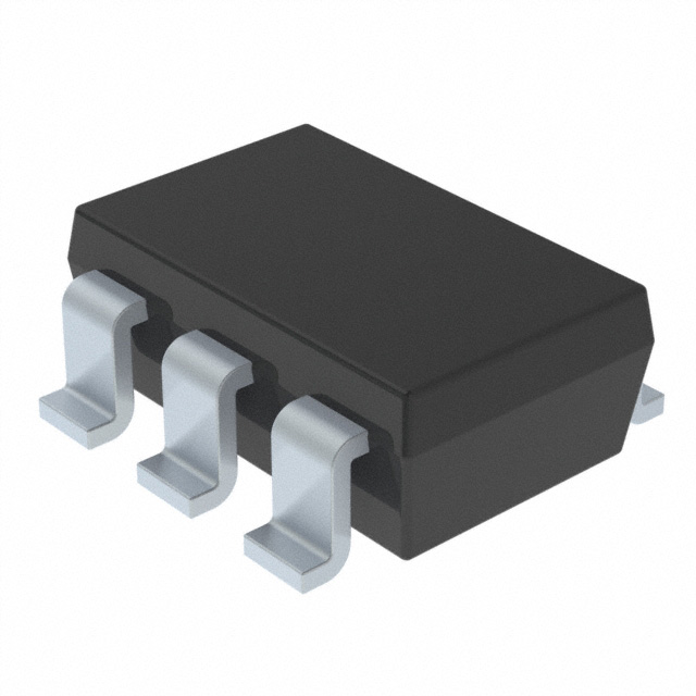
The AP1680 is available in SOT-23-6 package.
AP1680
Primary Side Control for Rectangular Constant
Current and Constant Voltage Output
Sub-microampere Start-up Current
30mW No-load Input Power Feasible
Tight CC Regulation Performance
Eliminates Opto-coupler and Secondary CV/CC
Control Circuitry
Eliminates Control Loop Compensation Circuitry
Flyback Topology in DCM Operation
Random Frequency Modulation to Reduce
System EMI
Built-in Soft Start
Open Feedback Protection
Short Circuit Protection
SOT-23-6 Package
Applications
·
·
·
LED Drivers
Adapters/Chargers for Cell/Cordless Phones,
PDAs, MP3 and Other Portable Apparatus
Standby and Auxiliary Power Supplies
SOT-23-6
Figure 1. Package Type of AP1680
Apr. 2011 Rev. 1. 0
BCD Semiconductor Manufacturing Limited
1
�Preliminary Datasheet
LOW-POWER OFF-LINE PRIMARY SIDE REGULATION CONTROLLER
AP1680
Pin Configuration
K6 Package
(SOT-23-6)
Pin 1 Dot by Marking
OUT
1
6
FB
GND
2
5
GND
VCC
3
4
CS
Figure 2. Pin Configuration of AP1680 (Top View)
Pin Description
Pin Number
Pin Name
Function
1
OUT
This pin drives the base of external power NPN switch
2, 5
GND
Ground
3
VCC
Supply voltage
4
CS
The primary current sense
6
FB
The voltage feedback from the auxiliary winding
Apr. 2011 Rev. 1. 0
BCD Semiconductor Manufacturing Limited
2
�Preliminary Datasheet
LOW-POWER OFF-LINE PRIMARY SIDE REGULATION CONTROLLER
AP1680
Functional Block Diagram
VCC
3
FB
6
0.1V
COMP
pfm
Tonsec
Detector
Regulator
&
Bias
Tons
UVLO
OCkP
EA
4.0V
CV_ctrl
R
Constant Voltage Control
Q
pfm
Driver 1
OUT
S
CS
4
Peak Current Control & LEB
Tons
Constant Current Control
R
Q
CC_ctrl
2, 5
GND
S
Figure 3. Functional Block Diagram of AP1680
Apr. 2011 Rev. 1. 0
BCD Semiconductor Manufacturing Limited
3
�Preliminary Datasheet
LOW-POWER OFF-LINE PRIMARY SIDE REGULATION CONTROLLER
AP1680
Ordering Information
AP1680
-
Circuit Type
G1: Green
Package
K6: SOT-23-6
Package
Temperature Range
SOT-23-6
-40 to 105oC
TR: Tape and Reel
Part Number
AP1680K6TR-G1
Marking ID
GBF
Packing Type
Tape & Reel
BCD Semiconductor's products, as designated with "G1" suffix in the part number, are RoHS compliant and Green.
Absolute Maximum Ratings (Note 1)
Parameter
Value
Unit
Supply Voltage VCC
-0.3 to 36
V
Voltage at CS, OUT to GND
-0.3 to 7
V
FB Input
-40 to 10
V
Internally limited
A
Output Current at OUT
Operating Junction Temperature
150
Storage Temperature
oC
-65 to 150
o
C
Lead Temperature (Soldering, 10s)
300
o
C
Thermal Resistance Junction-to-Ambient
250
ESD (Machine Model)
200
V
ESD (Human Body Model)
2000
V
o
C/W
Note 1: Stresses greater than those listed under "Absolute Maximum Ratings" may cause permanent damage to the device.
These are stress ratings only, and functional operation of the device at these or any other conditions beyond those indicated
under "Recommended Operating Conditions" is not implied. Exposure to "Absolute Maximum Ratings" for extended periods
may affect device reliability.
Apr. 2011 Rev. 1. 0
BCD Semiconductor Manufacturing Limited
4
�Preliminary Datasheet
LOW-POWER OFF-LINE PRIMARY SIDE REGULATION CONTROLLER
AP1680
Electrical Characteristics
(VCC=15V, TA=25oC, unless otherwise specified.)
Parameter
Symbol
Conditions
Min
Typ
Max
Unit
VTH (ST)
16
18.5
21
V
VOPR(min)
7.2
9
10.2
V
0.6
µA
200
320
µA
24
30
36
455
510
545
mV
3
%
455
mV
UVLO SECTION
Start-up Threshold
Minimal Operating Voltage
STANDBY CURRENT SECTION
IST
Start-up Current
Operating Current
ICC(OPR)
VCC=VTH (ST)-0.5V,
Before start-up
Static
DRIVE OUTPUT SECTION
OUT Maximum Current
Sink
Source
50
IOUT
mA
CURRENT SENSE SECTION
Current Sense Threshold
VCS
Equivalent Current Sense Voltage Accuracy
∆ Vcs, eq
Vcs, eq
Pre-Current Sense
VCS(PRE)
Note 2
365
Leading Edge Blanking
410
750
ns
FEEDBACK INPUT SECTION
Feedback Pin Input Leakage Current
IFB
Feedback Threshold
VFB
Note 2: The output current is given by IOUT=
VFB=4V
2.0
2.5
3.1
µA
3.59
3.83
4.07
V
Vcs, eq Np
xx .
Rcs
Ns
Apr. 2011 Rev. 1. 0
BCD Semiconductor Manufacturing Limited
5
�Preliminary Datasheet
LOW-POWER OFF-LINE PRIMARY SIDE REGULATION CONTROLLER
AP1680
Typical Performance Characteristics
10.5
Minimal Operating Voltage (V)
21
Start-up Voltage (V)
20
19
18
17
16
-40
-20
0
20
40
60
80
100
10.0
9.5
9.0
8.5
8.0
7.5
-40
120
-20
0
o
Ambient Temperature ( C)
20
40
60
80
100
120
o
Ambient Temperature ( C)
Figure 5. Mininal Operating Voltage vs.
Ambient Temperature
Figure 4. Start-up Voltage vs. Ambient Temperature
6
300
280
5
240
4
220
IFB (µA)
Operating Current (µA)
260
200
3
180
2
160
140
1
120
100
-40
-20
0
20
40
60
80
100
0
-40
120
-20
0
20
40
60
80
100
120
o
o
Ambient Temperature ( C)
Ambient Temperature ( C)
Figure 7. IFB vs. Ambient Temperature
Figure 6. Operating Current vs. Ambient Temperature
Apr. 2011 Rev. 1. 0
BCD Semiconductor Manufacturing Limited
6
�Preliminary Datasheet
LOW-POWER OFF-LINE PRIMARY SIDE REGULATION CONTROLLER
AP1680
Typical Application
D2
T1
V O+
+
C1
R1
+
C2
R5
D1
C3
NP
V
D3
R2
VCC
OUT
R3
Ns
C4 +
VO-
N FB
V
Q1
R6
AP1680
CS
R4
FB
GND
R7
Rs
Figure 8. 16.5V/350mA Output for LED Driver
Apr. 2011 Rev. 1. 0
BCD Semiconductor Manufacturing Limited
7
�Preliminary Datasheet
LOW-POWER OFF-LINE PRIMARY SIDE REGULATION CONTROLLER
AP1680
Mechanical Dimensions
SOT-23-6
Unit: mm(inch)
0°
2.820(0.111)
8°
3.020(0.119)
0.300(0.012)
0.400(0.016)
5
0.300(0.012)
0.600(0.024)
4
1.500(0.059)
1.700(0.067)
2.650(0.104)
2.950(0.116)
6
0.200(0.008)
Pin 1 Dot by Marking
1
2
3
0.700(0.028)REF
0.950(0.037)TYP
0.000(0.000)
0.150(0.006)
1.800(0.071)
2.000(0.079)
0.100(0.004)
0.200(0.008)
0.900(0.035) 1.450(0.057)
MAX
1.300(0.051)
Apr. 2011 Rev. 1. 0
BCD Semiconductor Manufacturing Limited
8
�BCD Semiconductor Manufacturing Limited
http://www.bcdsemi.com
IMPORTANT NOTICE
IMPORTANT
NOTICE
BCD Semiconductor
BCD
Semiconductor Manufacturing
Manufacturing Limited
Limited reserves
reserves the
the right
right to
to make
make changes
changes without
without further
further notice
notice to
to any
any products
products or
or specifispecifications herein.
cations
herein. BCD
BCD Semiconductor
Semiconductor Manufacturing
Manufacturing Limited
Limited does
does not
not assume
assume any
any responsibility
responsibility for
for use
use of
of any
any its
its products
products for
for any
any
particular purpose,
particular
purpose, nor
nor does
does BCD
BCD Semiconductor
Semiconductor Manufacturing
Manufacturing Limited
Limited assume
assume any
any liability
liability arising
arising out
out of
of the
the application
application or
or use
use
of any
of
any its
its products
products or
or circuits.
circuits. BCD
BCD Semiconductor
Semiconductor Manufacturing
Manufacturing Limited
Limited does
does not
not convey
convey any
any license
license under
under its
its patent
patent rights
rights or
or
other rights
other
rights nor
nor the
the rights
rights of
of others.
others.
MAIN SITE
SITE
MAIN
- Headquarters
BCD
Semiconductor Manufacturing Limited
BCD
Semiconductor
Manufacturing Limited
- Wafer
Fab
No.
1600, Zi
Xing Road,
Shanghai ZiZhu
Science-basedLimited
Industrial Park, 200241, China
Shanghai
SIM-BCD
Semiconductor
Manufacturing
Tel:
Fax: +86-21-24162277
800,+86-21-24162266,
Yi Shan Road, Shanghai
200233, China
Tel: +86-21-6485 1491, Fax: +86-21-5450 0008
REGIONAL SALES OFFICE
Shenzhen OfficeSALES OFFICE
REGIONAL
- Wafer
FabSemiconductor Manufacturing Limited
BCD
Shanghai
SIM-BCD
Semiconductor Manufacturing Co., Ltd.
- IC Design
Group
800 Yi
Shan Road,
Shanghai
200233,
China Corporation
Advanced
Analog
Circuits
(Shanghai)
Tel: +86-21-6485
1491,YiFax:
0008200233, China
8F, Zone B, 900,
Shan+86-21-5450
Road, Shanghai
Tel: +86-21-6495 9539, Fax: +86-21-6485 9673
Taiwan Office
Shanghai
Semiconductor Manufacturing Co., Ltd., Shenzhen Office
BCD Taiwan
Semiconductor
Shenzhen SIM-BCD
Office
Office (Taiwan) Company Limited
Unit
A Room
1203, Skyworth
Bldg., Gaoxin
Ave.1.S., Nanshan
Shenzhen,
4F, 298-1,
Guang Road,(Taiwan)
Nei-Hu District,
Taipei,
Shanghai
SIM-BCD
Semiconductor
Manufacturing
Co., Ltd.District,
Shenzhen
Office
BCDRui
Semiconductor
Company
Limited
China
Taiwan
Advanced Analog Circuits (Shanghai) Corporation Shenzhen Office
4F, 298-1, Rui Guang Road, Nei-Hu District, Taipei,
Tel:
+86-755-8826
Tel: +886-2-2656
2808
Room
E, 5F, Noble 7951
Center, No.1006, 3rd Fuzhong Road, Futian District, Shenzhen 518026, China
Taiwan
Fax:
+86-755-88267951
7865
Fax: +886-2-2656
28062808
Tel: +86-755-8826
Tel: +886-2-2656
Fax: +86-755-8826 7865
Fax: +886-2-2656 2806
USA Office
BCD Office
Semiconductor Corp.
USA
30920Semiconductor
Huntwood Ave.Corporation
Hayward,
BCD
CA 94544,
USA Ave. Hayward,
30920
Huntwood
Tel :94544,
+1-510-324-2988
CA
U.S.A
Fax:: +1-510-324-2988
+1-510-324-2788
Tel
Fax: +1-510-324-2788
�


 工商网监
湘ICP备2023018690号
工商网监
湘ICP备2023018690号
