Data Sheet
WHITE LED STEP-UP CONVERTER
AP3009
General Description
Features
The AP3009 is an inductor-based DC/DC converter
designed to drive up to six white LEDs in series for
backlight. Only one feedback resistor is needed to control the LED current and obtain satisfied brightness.
·
·
·
·
·
·
·
·
A constant frequency 1.2MHz PWM control scheme is
employed in this IC, which means the tiny external
components can be used. In fact, 1mm tall inductor and
0.22µF output capacitor for the typical application is
very appropriate. Additionally, the schottky diode in
boost circuit is integrated in this chip. AP3009 also
provide a disable port to ease its use for different systems.
Inherently Uniform LED Current
High Efficiency: 83% Typical
No Need for Extra Schottky Diode
Over Output Voltage Protection
Drives 2 to 6 LEDs
Fast 1.2MHz Switching Frequency
Uses Tiny 1mm Tall Inductor
Requires Only 0.22µF Output Capacitor
Applications
·
·
·
·
·
The over output voltage protection is equipped in
AP3009. When any LED is broken or in other abnormal conditions, the output voltage will be clamped to
30V.
Cellular Phones
Digital Cameras
LCD modules
GPS Receivers
PDAs, Handheld Computers
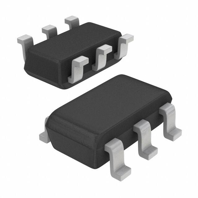
The AP3009 is available in standard SOT-23-6 package.
SOT-23-6
Figure 1. Package Type of AP3009
May 2013 Rev. 2. 0
BCD Semiconductor Manufacturing Limited
1
�Data Sheet
WHITE LED STEP-UP CONVERTER
AP3009
Pin Configuration
K Package
(SOT-23-6)
Pin 1 Mark
VOUT
1
6
SW
GND
2
5
VIN
FB
3
4
CTRL
Figure 2. Pin Configuration of AP3009 (Top View)
Pin Description
Pin Number
Pin Name
Function
1
VOUT
Output Pin. Connected to the cathode of internal schottky diode
2
GND
Ground Pin
3
FB
4
CTRL
5
VIN
Input Supply Pin. Must be locally bypassed
6
SW
Switch Pin. Connect external inductor
Voltage Feedback. Reference voltage is 200mV
Shutdown and Dimming Pin. Connect to 1.8V or higher to enable device; Connect to 50mV or
less to disable device; Connect to a voltage between 1.8V and 50mV to achieve linear dimming
May 2013 Rev. 2. 0
BCD Semiconductor Manufacturing Limited
2
�Data Sheet
WHITE LED STEP-UP CONVERTER
AP3009
Functional Block Diagram
FB
SW
3
VIN
5
VREF
1.25 V
6
200 mV
1
OVP
DRIVER
A1
A2
Q
R
VOUT
Q1
S
COMPARATOR
Σ
CTRL
2
4
GND
RAMP
GENERATOR
1.2 MHz
OSCILLATOR
Figure 3. Functional Block Diagram of AP3009
Ordering Information
AP3009
-
Circuit Type
E1: RoHS
Package
TR: Tape and Reel
K: SOT-23-6
Package
SOT-23-6
Temperature Range
o
-40 to 85 C
Part Number
AP3009KTR-E1
Marking ID
E9T
Packing Type
Tape & Reel
BCD Semiconductor's products as designated with "E1" suffix in the part number are RoHS compliant.
May 2013 Rev. 2. 0
BCD Semiconductor Manufacturing Limited
3
�Data Sheet
WHITE LED STEP-UP CONVERTER
AP3009
Absolute Maximum Ratings (Note 1)
Parameter
Symbol
Value
Unit
VIN
20
V
SW Voltage
38
V
FB Voltage
20
V
CTRL Voltage
20
V
265
oC/W
150
oC
TSTG
-65 to 150
oC
TLEAD
260
oC
ESD (Machine Model)
250
V
ESD (Human Body Model)
2000
V
Input Voltage
θJA
Thermal Resistance (Junction to Atmosphere, no Heat sink)
Operating Junction Temperature
Storage Temperature Range
Lead Temperature (Soldering, 10sec)
Note 1: Stresses greater than those listed under "Absolute Maximum Ratings" may cause permanent damage to the
device. These are stress ratings only, and functional operation of the device at these or any other conditions beyond those indicated under "Recommended Operating Conditions" is not implied. Exposure to "Absolute Maximum Ratings" for extended
periods may affect device reliability.
Recommended Operating Conditions
Parameter
Symbol
Min
Max
Unit
Operating Temperature Range
TOP
-40
85
oC
Input Voltage
VIN
2.5
16
V
CTRL Voltage
VCTRL
16
V
May 2013 Rev. 2. 0
BCD Semiconductor Manufacturing Limited
4
�Data Sheet
WHITE LED STEP-UP CONVERTER
AP3009
Electrical Characteristics
(VIN=3V, VCTRL =3V, TA=25oC, unless otherwise specified.)
Parameter
Symbol
Minimum Operating Voltage
VIN(min)
Maximum Operating Voltage
VIN(max)
Conditions
Min
Typ
Max
Unit
2.5
V
16
IOUT=20mA, 4 LEDs,
Feedback Voltage
VFB
FB Pin Bias Current
IFB
Supply Current
ICC
V FB=VIN, Not Switching
Supply Current
IQ
V CTRL=0V
Switching Frequency
200
212
mV
35
100
nA
1.9
2.6
3.3
mA
2.0
3.2
5.0
µA
f
0.8
1.2
1.6
MHz
Maximum Duty Cycle
DMAX
90
93
Switch Current Limit (Note 2)
ILIMIT
Switch VCE Saturation Voltage
VCESAT
Switch Leakage Current
CTRL Pin Voltage
VCTRL
TA=-40oC to 85oC
188
TA=25oC, D=40%
560
TA=25oC, D=80%
465
ISW=250mA
300
V SW=5V
0.01
High
Schottky Forward Drop
ICTRL
VDROP
5
µA
V
48
60
72
TA=85oC
40
50
60
TA=-40oC
60
75
90
ID=150mA
0.7
µA
V
4
V R=30V
Thermal Resistance
(Junction to Case)
mV
0.05
V R=25V
Schottky Leakage Current
mA
1.8
Low
CTRL Pin Bias Current
%
µA
90
θJC
60.84
oC/W
Note 2: The Switch Current Limit is related to Duty Cycle. Please refer to Figure 16 for detail.
May 2013 Rev. 2. 0
BCD Semiconductor Manufacturing Limited
5
�Data Sheet
WHITE LED STEP-UP CONVERTER
AP3009
Typical Performance Characteristics
85
85
84
84
Efficiency (%)
Efficiency (%)
(VF of WLED is 3.45V @ IF=20mA, unless otherwise noted )
83
82
83
82
o
VIN=3.6V, IOUT=20mA, 4 LEDs
CIN=1µF, COUT=0.22µF, L=22µH
81
80
-50
-25
0
25
50
75
4 LEDs, IOUT=20mA, TA=25 C
CIN=1µF, COUT=0.22µF, L=22µH
81
80
2.5
100
3.0
o
Figure 4. Efficiency vs. Junction Temperature
4.0
4.5
5.0
Figure 5. Efficiency vs. Input Voltage
86
Schottky Forward Current (mA)
350
84
Efficiency (%)
3.5
Input Voltage (V)
Junction Temperature ( C)
82
80
o
VIN=3.6V, IOUT=20mA, TA=25 C
CIN=1µF, COUT=0.22µF, L=22µH
78
3
4
5
250
200
150
100
50
76
2
300
0
6
0
LEDs (pcs)
200
400
600
800
1000
Schottky Forward Drop (mV)
Figure 6. Efficiency vs. LED's Number
Figure 7. Schottky Forward Current
vs. Schorttky Forward Drop
May 2013 Rev. 2. 0
BCD Semiconductor Manufacturing Limited
6
�Data Sheet
WHITE LED STEP-UP CONVERTER
AP3009
Typical Performance Characteristics (Continued)
(VF of WLED is 3.45V @ IF=20mA, unless otherwise noted )
3.5
3.0
25
Supply Current (mA)
Shutdown Quiescent Current (µA)
30
20
15
10
5
2.5
2.0
1.5
o
1.0
25 C
o
100 C
o
-50 C
0.5
0.0
0
4
6
8
10
12
14
0
16
2
4
Input Voltage (V)
Figure 8. Shutdown Quiescent Current vs. Input Voltage
8
10
12
14
16
Figure 9. Supply Current vs. Input Voltage
5.0
Input Current in Ouput Open Circuit (mA)
32.0
31.5
Output Clamp Voltage (V)
6
Input Voltage (V)
31.0
30.5
30.0
29.5
29.0
28.5
4
6
8
10
12
14
4.6
4.4
4.2
4.0
3.8
3.6
3.4
3.2
2.5
28.0
2
4.8
16
3.0
3.5
4.0
4.5
5.0
Input Voltage (V)
Input Voltage (V)
Figure 10. Output Clamp Voltage vs. Input Voltage
Figure 11. Input Current in Output Open Circuit
vs. Input Voltage
May 2013 Rev. 2. 0
BCD Semiconductor Manufacturing Limited
7
�Data Sheet
WHITE LED STEP-UP CONVERTER
AP3009
Typical Performance Characteristics (Continued)
1.25
202
1.20
201
Feedback Voltage (mV)
Switching Frequency (MHz)
(VF of WLED is 3.45V @ IF=20mA, unless otherwise noted )
1.15
1.10
1.05
1.00
0.95
-50
200
199
198
197
-25
0
25
50
75
196
-50
100
-25
o
0
25
50
Figure 13. Feedback Voltage
vs. Junction Temperature
vs. Junction Temperature
1.0
0.80
VR=10V
VR=16V
VR=25V
Schottky Leakage Current (uA)
Schottky Forward Drop (V)
0.78
0.76
0.74
0.72
0.70
0.68
0.66
0.64
0.60
-50
100
Junction Temperature ( C)
Figure 12. Switching Frequency
0.62
75
o
Junction Temperature ( C)
0.8
0.6
0.4
0.2
ID=150mA
-25
0
25
50
75
0.0
-50
100
o
-25
0
25
50
75
100
o
Junction Temperature ( C)
Junction Temperature ( C)
Figure 14. Schottky Forward Drop
vs. Junction Temperature
Figure 15. Schottky Leackage Current
vs. Junction Temperature
May 2013 Rev. 2. 0
BCD Semiconductor Manufacturing Limited
8
�Data Sheet
WHITE LED STEP-UP CONVERTER
AP3009
Typical Performance Characteristics (Continued)
(VF of WLED is 3.45V @ IF=20mA, unless otherwise noted )
400
700
o
Switching Current Limit (mA)
600
Switch Saturation Voltage (mV)
-50 C
o
25 C
o
100 C
500
400
300
200
100
30
40
50
60
70
80
90
350
300
250
200
150
100
50
50
100
100
150
200
250
300
Switch Current (mA)
Duty Cycle (%)
Figure 17. Switch Saturation Voltage
Figure 16. Switch Current Limit vs. Duty Cycle
vs. Switch Current
250
Feedback Voltage (mV)
200
150
100
50
0
0.0
0.5
1.0
1.5
2.0
CTRL Pin Voltage (V)
Figure 18. Feedback Voltage vs. CTRL Pin Voltage
May 2013 Rev. 2. 0
BCD Semiconductor Manufacturing Limited
9
�Data Sheet
WHITE LED STEP-UP CONVERTER
AP3009
Typical Application
VIN ≥ 3V
22µΗ
6
5
Control
Signal
4
VIN
1
SW
V OUT
AP3009
CTRL
0.22µF
FB
GND
1µF
3
10Ω
2
a. Four White LEDs Driver
VIN ≥ 3V
22µΗ
1
6
5
Control
Signal
4
1µF
VIN
SW
VOUT
AP3009
CTRL
GND
0.22µF
FB
3
10Ω
2
b. Five White LEDs Driver
May 2013 Rev. 2. 0
BCD Semiconductor Manufacturing Limited
10
�Data Sheet
WHITE LED STEP-UP CONVERTER
AP3009
Typical Application (Continued)
VIN ≥ 3V
22µΗ
6
5
Control
Signal
4
1µF
VIN
1
SW
VOUT
AP3009
CTRL
GND
0.22µF
FB
3
10Ω
2
c. Six White LEDs Driver
C: X5R or X7R Dielectric
L: SUMIDA CDRH5D28R-220NC or Equivalent
All these circuits can work in full temperature
Figure 19. Typical White LED Drivers
May 2013 Rev. 2. 0
BCD Semiconductor Manufacturing Limited
11
�Data Sheet
WHITE LED STEP-UP CONVERTER
AP3009
Mechanical Dimensions
SOT-23-6
Unit: mm(inch)
0°
2.820(0.111)
8°
3.100(0.122)
0.300(0.012)
0.500(0.020)
5
4
2
3
0.300(0.012)
0.600(0.024)
1.500(0.059)
1.700(0.067)
2.650(0.104)
3.000(0.118)
6
0.200(0.008)
Pin 1 Mark
1
0.700(0.028)REF
0.950(0.037)TYP
0.000(0.000)
0.150(0.006)
1.800(0.071)
2.000(0.079)
0.100(0.004)
0.200(0.008)
0.900(0.035) 1.450(0.057)
MAX
1.300(0.051)
May 2013 Rev. 2. 0
BCD Semiconductor Manufacturing Limited
12
�Data Sheet
WHITE LED STEP-UP CONVERTER
AP3009
Mounting Pad Layout
SOT-23-6
E
E
Y
G
Z
X
Dimensions
Z
(mm)/(inch)
G
(mm)/(inch)
X
(mm)/(inch)
Y
(mm)/(inch)
E
(mm)/(inch)
Value
3.600/0.142
1.600/0.063
0.700/0.028
1.000/0.039
0.950/0.037
May 2013 Rev. 2. 0
BCD Semiconductor Manufacturing Limited
13
�BCD Semiconductor Manufacturing Limited
http://www.bcdsemi.com
IMPORTANT NOTICE
BCD Semiconductor Manufacturing Limited reserves the right to make changes without further notice to any products or specifications herein. BCD Semiconductor Manufacturing Limited does not assume any responsibility for use of any its products for any
IMPORTANT NOTICE
IMPORTANT
NOTICE
particular purpose, nor does BCD Semiconductor Manufacturing Limited assume any liability arising out of the application or use
of any its products or circuits. BCD Semiconductor Manufacturing Limited does not convey any license under its patent rights or
BCD Semiconductor
BCD
Semiconductor Manufacturing
Manufacturing Limited
Limited reserves
reserves the
the right
right to
to make
make changes
changes without
without further
further notice
notice to
to any
any products
products or
or specifispecifiother rights nor the rights of others.
cations herein.
cations
herein. BCD
BCD Semiconductor
Semiconductor Manufacturing
Manufacturing Limited
Limited does
does not
not assume
assume any
any responsibility
responsibility for
for use
use of
of any
any its
its products
products for
for any
any
particular
particular
purpose,
purpose,
nor
nor
does
does
BCD
BCD
Semiconductor
Semiconductor
Manufacturing
Manufacturing
Limited
Limited
assume
assume
any
any
liability
liability
arising
arising
out
out
of
of
the
the
application
application
or
or
use
use
MAIN SITE
ofHeadquarters
any its
any
its products
products or
or circuits.
circuits. BCD
BCD Semiconductor
Semiconductor Manufacturing
Manufacturing
Limited
does not
does
not convey
convey any
any license
license under
under its
its patent
patent rights
rights or
or
-of
- Wafer Limited
Fab
BCD
(Shanghai)
Shanghai SIM-BCD Semiconductor Manufacturing Co., Ltd.
other
other
rights Micro-electronics
rights
nor the
nor
the rights
rightsLimited
of others.
of
others.
No. 1600, Zi Xing Road, Shanghai ZiZhu Science-based Industrial Park, 200241, P. R.C.
Tel: +86-021-2416-2266, Fax: +86-021-2416-2277
MAIN SITE
SITE
MAIN
REGIONAL
SALES Manufacturing
OFFICE
- Headquarters
BCD
Semiconductor
Limited
800 Yishan Road, Shanghai 200233, China
Tel: +021-6485-1491, Fax: +86-021-5450-0008
- Wafer
FabSemiconductor Manufacturing Limited
BCD
BCD
Semiconductor
Manufacturing Limited
Shanghai
SIM-BCD
Semiconductor Manufacturing Co., Ltd.
Shenzhen
Office
Taiwan
Office
(Taipei)
- Wafer
Fab
- IC Design
Group
No.
1600, Zi
Xing Road,
Shanghai ZiZhu
Science-basedCo.,
Industrial
Park, 200241,
China
Yi
Shan Road,
Shanghai
200233,
China
Shanghai
SIM-BCD
Semiconductor
Manufacturing
Ltd., Shenzhen
Office
BCD800
Semiconductor
(Taiwan)
Company
Limited
Shanghai
SIM-BCD
Semiconductor
Manufacturing
Limited
Advanced
Analog
Circuits
(Shanghai)
Corporation
Tel:
Fax: +86-21-24162277
Tel: +86-21-6485
1491,
0008Dist.,
Unit
A
1203,Skyworth
Bldg.,
Gaoxin
3F, No.17,
Lane
171,
Sec.
2,
Jiu-Zong
Rd.,Shanghai
Nei-Hu
Taipei(114),
Taiwan, R.O.C
800,+86-21-24162266,
YiRoom
Shan Road,
Shanghai
200233,
ChinaAve.1.S., Nanshan District
8F,
Zone
B, 900,
YiFax:
Shan+86-21-5450
Road,
200233,
China
Shenzhen
518057,1491,
ChinaFax: +86-21-5450 0008
Tel: +886-2-2656
2808
Tel: +86-21-6485
Tel: +86-21-6495
9539, Fax: +86-21-6485 9673
REGIONAL
SALES OFFICE
Tel: +86-0755-8660-4900,
Fax: +86-0755-8660-4958
Fax: +886-2-2656-2806/26562950
Shenzhen OfficeSALES OFFICE
Taiwan Office
USA Office
REGIONAL
Shanghai
SIM-BCD
Semiconductor Manufacturing Co., Ltd., Shenzhen Office
Semiconductor
BCD Office
Semiconductor Corp.
Taiwan
Office
(Hsinchu)
USABCD
Office
Korea Office USA
Shenzhen
Office
Taiwan
Office (Taiwan) Company Limited
Unit
ASemiconductor
Room
1203, Skyworth
Gaoxin
Ave.1.S., Nanshan
Shenzhen,
4F,Semiconductor
298-1,
Guang
Road,(Taiwan)
Nei-Hu District,
Taipei,
30920Semiconductor
Huntwood
Ave.Corporation
Hayward,
BCD
(Taiwan)Bldg.,
Company
Limited
BCD
Corp.
BCD
Semiconductor
Limited Korea
office.
Shanghai
SIM-BCD
Semiconductor
Manufacturing
Co., Ltd.District,
Shenzhen
Office
BCDRui
Semiconductor
Company
Limited
BCD
China
Taiwan
CADigital-Empire
94544,
USA Ave.
8F,
No.176,Analog
Sec. 2, Gong-Dao
5th Road, Corporation
East District Shenzhen Office
48460
Kato
CARoad,
94538,
USA District,
Room
101-1112,
II, 486
Sin-dong,
Advanced
Circuits (Shanghai)
4F,Road,
298-1,Fremont,
Rui Guang
Nei-Hu
Taipei,
30920
Huntwood
Hayward,
Tel:
+86-755-8826
7951
+886-2-2656
2808
Tel
:94544,
+1-510-324-2988
HsinChu
300, Taiwan,
R.O.C 3rd Fuzhong Road, Futian District, Shenzhen 518026, China
Tel:Tel:
+1-510-668-1950
Yeongtong-Gu,
Suwon-city,
Gyeonggi-do, Korea
Room
E, City
5F, Noble
Center, No.1006,
Taiwan
CA
U.S.A
Fax:
+86-755-8826
7865
Fax:
+886-2-2656
2806
Fax:
+1-510-324-2788
Tel:
+886-3-5160181,
Fax:
+886-3-5160181
Fax:
+1-510-668-1990
Tel:
+82-31-695-8430
Tel: +86-755-8826 7951
Tel: +886-2-2656 2808
Tel : +1-510-324-2988
Fax: +86-755-8826 7865
Fax: +886-2-2656 2806
Fax: +1-510-324-2788
�