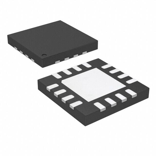
AP3156
HIGH EFFICIENCY 1X/1.5X/2X CHARGE PUMP
FOR WHITE LED APPLICATIONS
General Description
Features
•
•
•
•
•
•
•
•
•
•
•
•
•
•
The AP3156 is a low noise, constant frequency charge pump
DC/DC converter that uses a tri-mode load switch (1X), fractional
(1.5X), and doubling (2X) conversion to maximize efficiency for
white LED applications. The AP3156 is capable of driving the
LED channels at 120mA maximum from a 2.7V to 5.5V input. The
current sinks may be operated individually or in parallel for driving
higher-current LEDs. A low external parts count (two 1µF flying
capacitors and two small 1µF capacitors at VIN and VOUT) make
this part ideally suited for small, battery-powered applications.
VIN Range: 2.7V to 5.5V
Fully Programmable Current with Single Wire
• 32-Step Logarithmic Scale
• 20/25mA Max Current per Channel
• Four Low Current Settings Down to 50µA
• Low IQ (50µA) for Low Current Mode
Tri-Mode 1X, 1.5X, and 2X Charge Pump for Maximum
Efficiency and VF Coverage
Drives up to Six Channels of LEDs
Individual Main/Sub-Group Control
No Inductors, Low Noise Operation
0.5/1/2MHz Constant Switching Frequency
Small Application Circuit
Built-In Thermal Protection
Built-In Auto-Disable For Open Circuit
Automatic Soft Start
IQ 1MHz data rate), the LED current
drive of the AP3156 can be changed successively to brighten
or dim LEDs in smooth transitions or in abrupt steps, giving the
user complete programmability and real-time control of LED
brightness.
There are 32 current level settings separated from one another
by approximately 0.5dB (see Constant Current Programming
Level table). Code 1 is full-scale current, and Code 31 is full
scale attenuated roughly 15dB. Code 32 is reserved as a “no
current” setting.
Constant Current Programming Levels (mA)
20mA Max
25mA Max
Data
IOUT (mA)
IOUT (mA)
1
20
25
2
18.9
23.6
3
17.8
22.3
4
16.8
21.0
5
15.9
19.9
6
15.0
18.7
7
14.2
17.7
8
13.4
16.7
9
12.6
15.8
10
11.9
14.9
11
11.2
14.1
12
10.6
13.3
13
10.0
12.5
14
9.5
11.8
15
8.9
11.2
16
8.4
10.5
17
8.0
10.0
18
7.5
9.4
19
7.1
8.9
AP3156 Rev. 1
6.7
6.3
6.0
5.6
5.3
5.0
4.7
4.5
4.2
4.0
3.8
3.6
0
8.4
7.9
7.5
7.0
6.7
6.3
5.9
5.6
5.3
5.0
4.7
4.4
0
Low Current Output Level Setting
The AP3156 has a distinct Low Current mode with ultra-low
quiescent current. For drive currents of 2mA or less, the device
operates with significantly reduced quiescent current.
Low Current Programming Levels (mA)
Data
Current (mA)
1
2
2
1
3
0.5
4
0.05
5
0
Serial Digital Interface
SDI is a general purpose 1-wire digital interface designed to
transport digital controls for power management ICs such as
AP3156. The current levels of the six channels can be
configured either together, individually or specific grouping.
Up to 32 current levels are allowed. A generic system
controller can easily support the SDI protocol via bit-banging
over its general purpose I/Os.
The SDI protocol is simple yet flexible enough to
accommodate different switching clock frequencies. Any
sequence of negative-edged pulses of 63 or less (see
Instruction & Data Table) separated by TSEP at the SDI pin is
interpreted by the AP3156 as a channel configuration event.
In future, the number of pulses can be extended to support
additional commands.
9 of 15
www.diodes.com
SEPTEMBER 2009
© Diodes Incorporated
�AP3156
HIGH EFFICIENCY 1X/1.5X/2X CHARGE PUMP
FOR WHITE LED APPLICATIONS
Functional Description
Instruction & Data Table
First
Second
Sequence
Sequence
1~3
-
(Continued)
Description
No Action
Disabled Current Sinks
Unused current channels must be disabled by connecting the
sinks to VOUT with only a small sense current flowing through
the disabled channel.
4~7
1~32
8
1
Reserved
Switching frequency selected to
0.5MHz
2
Switching frequency selected to
1MHz (default)
3
Switching frequency selected to
2MHz
Short-Circuit Protection
Short-circuit protection function is incorporated to prevent
excessive load current when either flying cap terminals or
output pin electrically tied to a very lower voltage or ground.
4~32
1
Reserved
20mA Constant Current Mode,
32 current level supported
(default)
Over-Voltage Protection
Over-Voltage Protection function is incorporated to limit the
output voltage under a safe value to avoid on-chip device
breakdown.
2
Low Current Mode, 4 current level
supported
Under-Voltage Lockout
Under-Voltage lockout feature disables the device when the
input voltage drops below UVLO threshold.
3
25mA Constant Current Mode,
32 current level supported
4~32
Reserved
Set current level for all 6
Channels
Set current level for CH1, CH2,
CH3
Set current level for CH4, CH5,
CH6
Set current level for CH1, CH2,
CH3, CH4
Set current level for CH5, CH6
9
10
1~32*
11
1~32*
12
1~32*
13
1~32*
14
1~32*
15
1~32*
16
1~32*
Set current level for CH1, CH2,
CH3, CH4, CH5
Set current level for CH6
17
1~32*
Set current level for CH5
18
1~32*
Set current level for CH4
19
1~32*
Set current level for CH3
20
1~32*
Set current level for CH2
21
1~32*
Set current level for CH1
22~32
-
Reserved
33
-
34
-
Soft Reset
1) 1MHz switching frequency
2) 20mA Constant Current Mode
3) All Channels in Current Level
Setting 32 (0mA)
Null Sequence
35~63
Soft-Start
Soft-start is incorporated to prevent excessive inrush current
during power-up, mode switching, and transitioning out of
stand-by mode.
Thermal Auto Shutdown
When the die temperature exceeds the thermal limit, the
device will be disabled and enter stand-by mode. The
operation resumes whenever the die cools off sufficiently.
Switching frequency
By default, the AP3156 is working at 1MHz switching
frequency. It can also work at 0.5MHz or 2MHz switching
frequency which can be set through the Serial Digital Interface.
An user can choose the appropriate switching frequency with
consideration of noise immunity, input and output voltage
ripple requirement, and capacitor selection.
Reserved
* Only 1~5 are valid current settings at Low Current Mode.
AP3156 Rev. 1
10 of 15
www.diodes.com
SEPTEMBER 2009
© Diodes Incorporated
�AP3156
HIGH EFFICIENCY 1X/1.5X/2X CHARGE PUMP
FOR WHITE LED APPLICATIONS
Serial Digital Interface
SDI Command Timing Protocol
For the SDI command to be successfully received by the AP3156, all SDI timing specifications must be satisfied.
When no command is being sent, the SDI pin should be held High. If the SDI pin goes Low and stays Low for a time length between
TSLO(min) and TSLO(max) and then goes High and stays High for the length between TSHI(min) and TSHI(max), one falling edge is
registered by the AP3156. The total number of falling edges registered before the SDI pin is held High for longer than the maximum
separation time TSEP(max) identifies the command that has been received by the AP3156. The next series of falling edges before
another separation time of TSEP represents the next command. In other words, the AP3156 counts the number of consecutive falling
edges on the SDI pin and a different number represents a different command.
Each command is executed after it is successfully received. If at any time the SDI pin is held Low for longer than the maximum chip
disable time TOFF(max), then the AP3156 will be turned off and enters the shutdown mode. Setting the SDI pin switching from Low to High
will re-enable the AP3156 and leave the shutdown mode. If the SDI pin is held on for a time duration over TSEP, then an end of a
sequence (EOS) occurs with a number of pulse conformed to specified timing.
A valid dual-sequence command occurs when one valid sequence is defined as an instruction, and the other is defined as data. Both
sequences have number of pulses less than 33. Also, a valid single-sequence command occurs when the sequence has number of
pulses greater than 32.
First Sequence
TSHI
SDI
1
2
8
Second Sequence
TSLO
9
Channel Selection
TSEP
TSEP
10
1
2
Current Setting
Channel D1
Channel 1 in
dimming control
Set Channel 1 to current level 2.
Channel D2
Channel 2 in
dimming control
Set Channel 2 to current level 2.
Channel D3
Channel 3 in
dimming control
Set Channel 3 to current level 2.
Channel D4
Channel 4 in
dimming control
Set Channel 4 to current level 2.
Channel D5
Channel 5 in
dimming control
Set Channel 5 to current level 2.
Channel D6
Channel 6 in
dimming control
Set Channel 6 to current level 2.
Figure 1: Dimming Control Selection (Dual-Sequence Command)
AP3156 Rev. 1
11 of 15
www.diodes.com
SEPTEMBER 2009
© Diodes Incorporated
�AP3156
HIGH EFFICIENCY 1X/1.5X/2X CHARGE PUMP
FOR WHITE LED APPLICATIONS
Serial Digital Interface
(Continued)
Second Sequence
First Sequence
TSHI
TSLO
TSEP
TSEP
SDI
1
2
7
8
1
9
Current Mode Selection
2
Select Low Current Mode
Figure 2: Current Mode Selection (Dual-Sequence Command)
First Sequence
TSHI
Second Sequence
TSLO
TSEP
TSEP
SDI
1
2
6
7
8
1
Switching Frequency Selection
2
Select Switching Frequency
to 1 MHZ
Figure 3: Switching Frequency Selection (Dual-Sequence Command)
First Sequence
TSHI
TSLO
TSEP
SDI
1
2
31
32
33
Soft Reset
Figure 4: Soft Reset (Single-Sequence Command)
AP3156 Rev. 1
12 of 15
www.diodes.com
SEPTEMBER 2009
© Diodes Incorporated
�AP3156
HIGH EFFICIENCY 1X/1.5X/2X CHARGE PUMP
FOR WHITE LED APPLICATIONS
Marking Information
(1) QFN4040-16
( Top View )
XX : F7 : AP3156
Y : Year : 0~9
W : Week : A~Z : 1~26 week;
a~z : 27~52 week;
z represents 52 and 53 week
X : A~Z : Green
XX
YW X
Part Number
AP3156FVG-7
Package Information
Package
QFN4040-16
Identification Code
F7
(All Dimensions in mm)
(1) Package Type: QFN4040-16
CL
0.10 C
Seating Plane
B
C
0.15Max.
0.25 A
Side View
Land Pattern Recommendatrion
4
3.7
2X-
0.55/0.65
0.08 C
0.05Max.
16X-
3.90/4.10
A
10
4
1
3.7
0.55/0.65
4
2.3/2.5
3.90/4.10
2.3/2.5
(Pin #1 ID)
(Pin #1 ID)
16
0.25 B
0.65Typ.
0.28/0.38
0.10
C A B
Bottom View
AP3156 Rev. 1
16x-1.0
2X-
13 of 15
www.diodes.com
12x-0.65
Bottom View
SEPTEMBER 2009
© Diodes Incorporated
�AP3156
HIGH EFFICIENCY 1X/1.5X/2X CHARGE PUMP
FOR WHITE LED APPLICATIONS
Taping Orientation
Note:
(Note 8)
8. The taping orientation of the other package type can be found on our website at http://www.diodes.com/datasheets/ap02007.pdf
AP3156 Rev. 1
14 of 15
www.diodes.com
SEPTEMBER 2009
© Diodes Incorporated
�AP3156
HIGH EFFICIENCY 1X/1.5X/2X CHARGE PUMP
FOR WHITE LED APPLICATIONS
IMPORTANT NOTICE
DIODES INCORPORATED MAKES NO WARRANTY OF ANY KIND, EXPRESS OR IMPLIED, WITH REGARDS TO THIS
DOCUMENT, INCLUDING, BUT NOT LIMITED TO, THE IMPLIED WARRANTIES OF MERCHANTABILITY AND FITNESS FOR A
PARTICULAR PURPOSE (AND THEIR EQUIVALENTS UNDER THE LAWS OF ANY JURISDICTION).
Diodes Incorporated and its subsidiaries reserve the right to make modifications, enhancements, improvements, corrections or other
changes without further notice to this document and any product described herein. Diodes Incorporated does not assume any liability
arising out of the application or use of this document or any product described herein; neither does Diodes Incorporated convey any
license under its patent or trademark rights, nor the rights of others. Any Customer or user of this document or products described
herein in such applications shall assume all risks of such use and will agree to hold Diodes Incorporated and all the companies
whose products are represented on Diodes Incorporated website, harmless against all damages.
Diodes Incorporated does not warrant or accept any liability whatsoever in respect of any products purchased through unauthorized
sales channel.
Should Customers purchase or use Diodes Incorporated products for any unintended or unauthorized application, Customers shall
indemnify and hold Diodes Incorporated and its representatives harmless against all claims, damages, expenses, and attorney fees
arising out of, directly or indirectly, any claim of personal injury or death associated with such unintended or unauthorized application.
Products described herein may be covered by one or more United States, international or foreign patents pending. Product names
and markings noted herein may also be covered by one or more United States, international or foreign trademarks.
LIFE SUPPORT
Diodes Incorporated products are specifically not authorized for use as critical components in life support devices or systems without
the express written approval of the Chief Executive Officer of Diodes Incorporated. As used herein:
A. Life support devices or systems are devices or systems which:
1. are intended to implant into the body, or
2. support or sustain life and whose failure to perform when properly used in accordance with instructions for use provided
in the labeling can be reasonably expected to result in significant injury to the user.
B.
A critical component is any component in a life support device or system whose failure to perform can be reasonably expected
to cause the failure of the life support device or to affect its safety or effectiveness.
Customers represent that they have all necessary expertise in the safety and regulatory ramifications of their life support devices or
systems, and acknowledge and agree that they are solely responsible for all legal, regulatory and safety-related requirements
concerning their products and any use of Diodes Incorporated products in such safety-critical, life support devices or systems,
notwithstanding any devices- or systems-related information or support that may be provided by Diodes Incorporated. Further,
Customers must fully indemnify Diodes Incorporated and its representatives against any damages arising out of the use of Diodes
Incorporated products in such safety-critical, life support devices or systems.
Copyright © 2009, Diodes Incorporated
www.diodes.com
AP3156 Rev. 1
15 of 15
www.diodes.com
SEPTEMBER 2009
© Diodes Incorporated
�