PART OBSOLETE – NO ALTERNATE PART
AP3433
3A 2MHZ HIGH PERFORMANCE SYNCHRONOUS BUCK CONVERTER
Pin Assignments
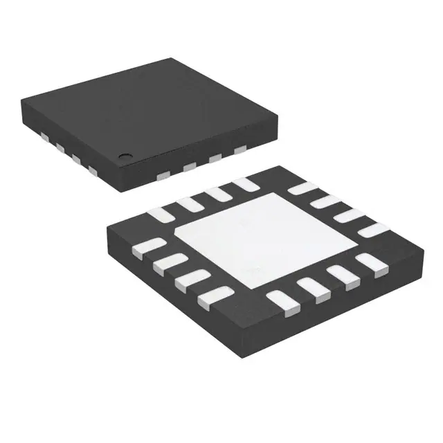
The AP3433 is available in QFN-3×3-16 package.
Input Voltage Range: 2.95V to 5.5V
0.827V Reference Voltage with ±3% Precision
Two 45mΩ(typical) MOSFETs for High Efficiency at 3A Load
High Efficiency: up to 94%
Output Current: 3A
Programmable Frequency:300kHz to 2MHz
Current Mode Control
Synchronizes to External Clock
Adjustable Soft-start
Soft Start-up into Pre-biased Output
UV and OV Power Good Output
Built-in Over Current Protection
Built-in Thermal Shutdown Function
Programmable UVLO Function
Built-in Over Voltage Protection
Thermally Enhanced 3mm×3mm 16-pin QFN
Document number: DS41485 Rev. 1 - 4
BOOT
13
SW
2
11
SW
10
SW
9
SS
3
GND
4
EP
5
6
7
8
QFN-3×3-16
Applications
Features
AP3433
14
12
GND
Under voltage lockout is internally set at 2.6V, but can be increased
by programming the threshold with a resistor network on the enable
pin. The output voltage startup ramp is controlled by the soft-start pin.
An open drain power good signal indicates the output is within 93% to
107% of its nominal voltage.
15
RT/CLK
VIN
The switching frequency of AP3433 can be programmable from
300kHz to 2MHz, which allows small-sized components, such as
capacitors and inductors. A standard series of inductors from several
different manufacturers are available. This feature greatly simplifies
the design of switch-mode power supplies.
16
1
COMP
VIN
PGD
Pin 1 Mark
FB
The device integrates two N-channel power MOSFETs with low onresistance. Current mode control provides fast transient response and
cycle-by-cycle current limit.
EN
(Top View)
VIN
OBSOLETE – PART DISCONTINUED
The AP3433 is a current mode, PWM synchronous buck (step-down)
DC-DC converter, capable of driving a 3A load with high efficiency,
excellent line and load regulation.
AGND
Description
Low-voltage, High-density Power Systems
Point of Load Regulation for Consumer Applications such as Set
Top Boxes, LCD Displays, CPE Equipment
1 of 11
www.diodes.com
October 2018
© Diodes Incorporated
�PART OBSOLETE – NO ALTERNATE PART
AP3433
Typical Applications Circuit
U1
VIN=5V
16
OBSOLETE – PART DISCONTINUED
1
C2
C3
C1
10mF 0.1mF
R4
R1 100kΩ
2
14
15
7
8
R2
9
L1 1.5mH
VIN
SW
VIN
SW
VIN
SW
EN
AP3433
12
C10 2.2nF
(Optional)
6
FB
GND
RT/CLK
GND
AGND
C6
0.1mF
13
COMP
SS
R8 2.2Ω
(Optional)
11
BOOT
PGD
VOUT=1.8V
10
R6
12kΩ
3
4
R7
10kΩ
C8
22mF
C9
22mF
5
R3
7.5kΩ
C5
Optional
C4
3.3nF
R5
180kΩ
C7
0.01mF
Pin Descriptions
Pin Number
Pin Name
Function
1,2,16
VIN
Supply input pin. A capacitor should be connected between the VIN and GND pin to keep the DC
input voltage constant
3,4
GND
Power ground. This pin should be electrically connected to the power pad under the IC
5
AGND
6
FB
7
COMP
Compensation pin. This pin is the output of the transconductance error amplifier and the input to the
current comparator. Connect external compensation elements to this pin to stabilize the control loop
8
RT/CLK
Resistor timing or external clock input pin
9
SS
Soft-start pin. An external capacitor connected to this pin sets the output voltage rise time. This pin
can also be used for tracking
10,11,12
SW
Internal power switch output pin. This pin is connected to the inductor and bootstrap capacitor
13
BOOT
14
PGD
15
EN
AP3433
Document number: DS41485 Rev. 1 - 4
Analog ground. This pin should be electrically connected to GND close to the device
Feedback pin. Inverting node of the transconductance error amplifier
Bootstrap pin. A bootstrap capacitor is connected between the BOOT pin and SW pin. The voltage
across the bootstrap capacitor drives the internal high-side power MOSFET
Power good indicator output. Asserts low if output voltage is low due to thermal shutdown, overcurrent, over/under-voltage or EN shut down
Enable pin, internal pull-up current source. Pull below 1.2V to disable. Float to enable. Can be used to
set the on/off threshold (adjust UVLO) with two additional resistors
2 of 11
www.diodes.com
October 2018
© Diodes Incorporated
�PART OBSOLETE – NO ALTERNATE PART
AP3433
OBSOLETE – PART DISCONTINUED
Functional Block Diagram
AP3433
Document number: DS41485 Rev. 1 - 4
3 of 11
www.diodes.com
October 2018
© Diodes Incorporated
�PART OBSOLETE – NO ALTERNATE PART
AP3433
Absolute Maximum Ratings (Note 1)
OBSOLETE – PART DISCONTINUED
Symbol
Parameter
Value
Unit
VIN
VIN Pin Voltage
-0.3 to 6.5
V
VEN
EN Pin Voltage
-0.3 to 6.5
V
VSW
SW Pin Voltage
-0.3 to VIN+0.3
V
VFB
FB Pin Voltage
-0.3 to 6.5
V
VCOMP
COMP Pin Voltage
-0.3 to 6.5
V
VPGD
PGD Pin Voltage
-0.3 to 6.5
V
RT/CLK Pin Voltage
-0.3 to 6.5
V
VSS
SS Pin Voltage
-0.3 to 6.5
V
θJA
Thermal Resistance
(Junction to Ambient)
Thermal Resistance
(Junction to Case)
70
ºC/W
5
ºC/W
Operating Junction Temperature
-40 to +125
ºC
TSTG
Storage Temperature
-65 to +150
ºC
TLEAD
Lead Temperature (Soldering, 10sec)
+260
ºC
_
ESD (Machine Model)
200
V
_
ESD (Human Body Model)
2000
V
VRT/CLK
θJC (BOTTOM)
TJ
Stresses greater than those listed under “Absolute Maximum Ratings” may cause permanent damage to the device. These are stress ratings only, and
Note 1:
functional operation of the device at these or any other conditions beyond those indicated under “Recommended Operating Conditions” is not implied.
Exposure to “Absolute Maximum Ratings” for extended periods may affect device reliability.
Recommended Operating Conditions
Symbol
VIN
IOUT(MAX)
TA
AP3433
Document number: DS41485 Rev. 1 - 4
Parameter
Min
Max
Unit
Input Voltage
2.95
5.5
V
3
_
A
-40
+85
ºC
Maximum Output Current
Operating Ambient Temperature
4 of 11
www.diodes.com
October 2018
© Diodes Incorporated
�PART OBSOLETE – NO ALTERNATE PART
Electrical Characteristics
AP3433
(VIN=2.95 to 5.5V, TA=25ºC, unless otherwise specified. Specifications with boldface type apply over full
operating temperature range from -40 to +85ºC.)
Symbol
Parameters
Conditions
Min
Typ
Max
Unit
_
2.95
_
5.5
V
_
360
575
μA
_
2
5
μA
Rising
1.16
1.25
1.37
V
Falling
_
1.18
_
V
_
_
2.6
2.8
V
_
_
150
_
mV
0.802
0.827
0.852
V
VBOOT-SW=5V
_
45
81
mΩ
VBOOT-SW=2.95V
_
64
110
mΩ
VIN=5V
_
42
81
mΩ
VIN=2.95V
_
59
110
mΩ
OBSOLETE – PART DISCONTINUED
SUPPLY VOLTAGE (VIN PIN)
VIN
Input Voltage
IQ
Quiescent Current
ISHDN
Shutdown Supply Current
VFB=0.9V,VIN=5V, TA=25C,
RT=400kΩ
VEN=0V,TA=25C
2.95V≤VIN≤5.5V
ENABLE AND UVLO (EN PIN)
VEN_H
VEN_L
VUVLO
VHYS
Enable Threshold
Internal Under Voltage Lockout
Threshold
Internal Under Voltage
Hysteresis
VOLTAGE REFERENCE (FB PIN)
VREF
Voltage Reference
2.95V≤VIN≤5.5V
MOSFET
RON_H
RON_L
High Side Switch On-resistance
Low Side Switch On-resistance
CURRENT LIMIT
ILIMIT
Current Limit Threshold
_
4.2
6.6
_
A
Thermal Shutdown
_
_
+140
_
C
Hysteresis
_
_
+20
_
C
THERMAL SHUTDOWN
TTSD
_
AP3433
Document number: DS41485 Rev. 1 - 4
5 of 11
www.diodes.com
October 2018
© Diodes Incorporated
�PART OBSOLETE – NO ALTERNATE PART
Electrical Characteristics
AP3433
(Cont. VIN=2.95 to 5.5V, TA=25ºC, unless otherwise specified. Specifications with boldface type apply
over full operating temperature range from -40 to +85ºC.)
Symbol
Parameters
Conditions
Min
Typ
Max
Unit
_
300
_
2000
kHz
_
300
_
2000
kHz
OBSOLETE – PART DISCONTINUED
TIMING RESISTOR AND EXTERNAL CLOCK (RT/CLK PIN)
_
_
Switching Frequency Range (RT
Mode)
Switching Frequency Range (CLK
Mode)
fS
Switching Frequency
RT=400kΩ
400
500
600
kHz
_
Minimum CLK Pulse Width
_
75
_
_
ns
_
RT/CLK Voltage
RT=400kΩ
_
0.5
_
V
_
RT/CLK High Threshold
_
_
1.6
2.2
V
_
RT/CLK Low Threshold
_
0.4
0.6
_
V
BOOT Charge Resistor
VIN=5V
_
16
_
Ω
BOOT-SW UVLO
VIN=2.95V
_
2.2
_
V
BOOT (BOOT PIN)
RBOOT
_
SOFT START (SS PIN)
ISS
Charge Current
VSS=0.4
_
2.2
_
μA
VSS
SS to Reference Crossover
98% Nominal
_
1.1
_
V
VFB Falling (Fault)
_
91
_
VFB Rising (Good)
_
93
_
VFB Rising (Fault)
_
107
_
VFB Falling (Good)
_
105
_
POWER GOOD (PGD PIN)
VFB TH
Feedback Threshold
AP3433
Document number: DS41485 Rev. 1 - 4
%VREF
6 of 11
www.diodes.com
October 2018
© Diodes Incorporated
�PART OBSOLETE – NO ALTERNATE PART
AP3433
Performance Characteristics
Supply Current vs. Input Voltage
Supply Current vs. Temperature
470
430
425
460
450
410
440
Supply Current (mA)
Supply Current (mA)
415
405
400
395
390
385
380
375
370
365
360
2.7
3.0
3.3
3.6
3.9
4.2
4.5
4.8
5.1
5.4
430
420
410
400
390
VIN=5V
380
VFB=0.9V
370
-50
5.7
-25
0
25
50
75
100
125
150
o
Input Voltage (V)
Temperature ( C)
Efficiency vs. Output Current
UVLO Threshold vs. Temperature
100
2.60
95
2.55
90
2.50
80
2.45
UVLO Threshold (V)
85
Efficiency (%)
75
70
65
60
55
VOUT=1.8V
50
45
VIN=3.3V
40
VIN=5V
2.40
2.35
2.30
2.25
2.20
Start Switching
Stop Switching
2.15
35
30
2.10
0
300
600
900
1200
1500
1800
2100
2400
2700
3000
-50
-25
0
25
50
75
100
125
150
o
Output Current (mA)
Temperature ( C)
Switching Frequency vs. Temperature
Reference Voltage vs. Temperature
1020
0.834
1010
0.832
1000
990
0.830
RT=180k
Reference Voltage (V)
Switching Frequency (kHz)
OBSOLETE – PART DISCONTINUED
420
980
970
960
950
940
930
0.828
0.826
0.824
0.822
0.820
920
910
0.818
900
-50
-25
0
25
50
75
100
125
150
o
Temperature ( C)
AP3433
Document number: DS41485 Rev. 1 - 4
0.816
-50
-25
0
25
50
75
100
125
150
Temperature (C)
7 of 11
www.diodes.com
October 2018
© Diodes Incorporated
�PART OBSOLETE – NO ALTERNATE PART
AP3433
Performance Characteristics (Cont.)
Switching Frequency vs. RT Resistance
Low Frequency Range
Switching Frequency vs. RT Resistance
High Frequency Range
2000
800
Switching Frequency (kHz)
Switching Frequency (kHz)
OBSOLETE – PART DISCONTINUED
1900
700
600
500
400
300
1800
1700
1600
1500
1400
1300
1200
1100
1000
200
900
100
300
400
500
600
700
800
900
800
80
1000
100
120
140
160
180
200
RT Resistance (k)
RT Resistance (k)
Start up from VIN (VIN=5V, VOUT=1.8V, IOUT=3A)
Disable IC (VIN=5V, VOUT=1.8V, IOUT=3A)
VEN
2V/div
VIN
2V/div
VOUT
1V/div
VOUT
1V/div
VSS
2V/div
VSS
2V/div
IL
2A/div
IL
2A/div
Time 4ms/div
Time 20μs/div
Load Transient Response
(VIN=5V, VOUT=1.8V, IOUT=0 to 3A)
VOUT(AC)
200mV/div
Synchronizing to External Clock
(fCLOCK=2MHz)
VCLOCK
2V/div
VSW
2V/div
IOUT
2A/div
Time 200μs/div
AP3433
Document number: DS41485 Rev. 1 - 4
Time 400ns/div
8 of 11
www.diodes.com
October 2018
© Diodes Incorporated
�PART OBSOLETE – NO ALTERNATE PART
AP3433
Performance Characteristics (Cont.)
OBSOLETE – PART DISCONTINUED
Short Circuit Protection
(VIN=5V, VOUT=1.8V, IOUT=3A)
VOUT
1V/div
Short Circuit Recovery
(VIN=5V, VOUT=1.8V, IOUT=3A)
VOUT
1V/div
VSS
2V/div
VSS
2V/div
VCOMP
0.5V/div
VCOMP
0.5V/div
IL
2A/div
IL
2A/div
Time 4ms/div
Time 4ms/div
Ordering Information
AP3433 XX XX - XX
Product Name
Package
Temperature
Range
QFN-3×3-16
-40 to +85ºC
AP3433
Document number: DS41485 Rev. 1 - 4
Package
Packing
RoHS/Green
FN : QFN-3x3-16
TR : Tape & Reel
G1 : Green
Part Number
AP3433FNTR-G1
9 of 11
www.diodes.com
Marking ID
Packing
B1D
Tape & Reel
October 2018
© Diodes Incorporated
�PART OBSOLETE – NO ALTERNATE PART
AP3433
Package Outline Dimensions (All dimensions in mm(inch).)
Package Type: QFN-3×3-16
OBSOLETE – PART DISCONTINUED
(1)
AP3433
Document number: DS41485 Rev. 1 - 4
10 of 11
www.diodes.com
October 2018
© Diodes Incorporated
�PART OBSOLETE – NO ALTERNATE PART
AP3433
IMPORTANT NOTICE
OBSOLETE – PART DISCONTINUED
DIODES INCORPORATED MAKES NO WARRANTY OF ANY KIND, EXPRESS OR IMPLIED, WITH REGARDS TO THIS DOCUMENT,
INCLUDING, BUT NOT LIMITED TO, THE IMPLIED WARRANTIES OF MERCHANTABILITY AND FITNESS FOR A PARTICULAR PURPOSE
(AND THEIR EQUIVALENTS UNDER THE LAWS OF ANY JURISDICTION).
Diodes Incorporated and its subsidiaries reserve the right to make modifications, enhancements, improvements, corrections or other changes
without further notice to this document and any product described herein. Diodes Incorporated does not assume any liability arising out of the
application or use of this document or any product described herein; neither does Diodes Incorporated convey any license under its patent or
trademark rights, nor the rights of others. Any Customer or user of this document or products described herein in such applications shall assume
all risks of such use and will agree to hold Diodes Incorporated and all the companies whose products are represented on Diodes Incorporated
website, harmless against all damages.
Diodes Incorporated does not warrant or accept any liability whatsoever in respect of any products purchased through unauthorized sales channel.
Should Customers purchase or use Diodes Incorporated products for any unintended or unauthorized application, Customers shall indemnify and
hold Diodes Incorporated and its representatives harmless against all claims, damages, expenses, and attorney fees arising out of, directly or
indirectly, any claim of personal injury or death associated with such unintended or unauthorized application.
Products described herein may be covered by one or more United States, international or foreign patents pending. Product names and markings
noted herein may also be covered by one or more United States, international or foreign trademarks.
This document is written in English but may be translated into multiple languages for reference. Only the English version of this document is the
final and determinative format released by Diodes Incorporated.
LIFE SUPPORT
Diodes Incorporated products are specifically not authorized for use as critical components in life support devices or systems without the express
written approval of the Chief Executive Officer of Diodes Incorporated. As used herein:
A. Life support devices or systems are devices or systems which:
1. are intended to implant into the body, or
2. support or sustain life and whose failure to perform when properly used in accordance with instructions for use provided in the
labeling can be reasonably expected to result in significant injury to the user.
B. A critical component is any component in a life support device or system whose failure to perform can be reasonably expected to cause the
failure of the life support device or to affect its safety or effectiveness.
Customers represent that they have all necessary expertise in the safety and regulatory ramifications of their life support devices or systems, and
acknowledge and agree that they are solely responsible for all legal, regulatory and safety-related requirements concerning their products and any
use of Diodes Incorporated products in such safety-critical, life support devices or systems, notwithstanding any devices- or systems-related
information or support that may be provided by Diodes Incorporated. Further, Customers must fully indemnify Diodes Incorporated and its
representatives against any damages arising out of the use of Diodes Incorporated products in such safety-critical, life support devices or systems.
Copyright © 2018, Diodes Incorporated
www.diodes.com
AP3433
Document number: DS41485 Rev. 1 - 4
11 of 11
www.diodes.com
October 2018
© Diodes Incorporated
�


 工商网监
湘ICP备2023018690号
工商网监
湘ICP备2023018690号

