PART OBSOLETE - NO ALTERNATE PART
AP3615
5 CHANNEL CHARGE PUMP CURRENT SINK FOR LED DRIVER
Pin Assignments
2
C2+
3
C1+
4
The supply voltage of AP3615 ranges from 2.8V to 5.5V which make
it ideally suit for applications powered by Li-ion battery.
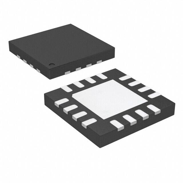
The AP3615 is available in the tiny package of QFN-3×3-16.
Regulated Output Current with ±3% Matching
Drives up to 5 WLEDs at 20mA Each
16 Steps Brightness Control Using Pulse Signal Dimming
Mobile Phone
Wide Operating Voltage Range: 2.8V to 5.5V
PDA
High Operating Frequency: 1MHz
MP3/4
Auto 1x/1.5x Charge Pump Mode Selection
Built-in Soft-start
Output Over Voltage Protection
Built-in UVLO
Built-in OTSD
Operating Temperature Range: -40°C to +85°C
Document number: DS41101 Rev. 3 - 4
5
6
7
8
D2
11
D3
10
D4
9
D5
Exposed PAD,
Connected to AGND
QFN-3×3-16
AP3615
EP
12
Note: Pin 14 should be connected with Pin 16 on PCB Board.
Features
13
EN
C2-
14
VIN
1
15
PGND
C1-
D1
16
The AP3615 provides up to 20mA current for each WLED. There are
totally 16 steps of current control, which is achieved through a digital
pulse dimming function on EN pin. Additionally, 1MHz high switching
frequency enables the use of small external capacitors. Internal softstart circuitry prevents excessive inrush current during start-up and
mode transition.
VOUT2
Pin 1 Mark
NC
(Top View)
VOUT1
OBSOLETE – PART DISCONTINUED
The AP3615 is a step-up DC-DC converter based on 1x/1.5x charge
pump and low dropout current sink, which helps it maintain the
highest efficiency. The AP3615 is specially designed to drive up to 5
WLEDs in backlight display.
AGND
Description
Applications
1 of 11
www.diodes.com
January 2019
© Diodes Incorporated
�PART OBSOLETE - NO ALTERNATE PART
AP3615
Typical Applications Circuit
OBSOLETE – PART DISCONTINUED
C2
1F
C1
1F
D1
7
Li-ion
Battery
CIN
1F
1
4
2
3
C1-
C1+
C2-
C2+
D1
EN
5
COUT
D2
AP3615
14
16
D3
D4
D4
D5
VIN
Pulse Input
8
D2
VOUT2
D3
VOUT1
D4
AGND
D5
PGND
1F
13
12
11
10
9
6
4 WLEDs
C1
C2
1F
1F
D1
7
Li-ion
Battery
CIN
1 F
1
4
2
3
C1-
C1+
C2-
C2+
VIN
D1
Pulse Input
8
14
16
COUT
5
EN
AP3615
D2
VOUT2
D3
VOUT1
D4
AGND
1F
PGND
D5
D2
D3
13
12
11
10
9
6
5 WLEDs
Detailed application information, please refer to AP3615 application note.
AP3615
Document number: DS41101 Rev. 3 - 4
2 of 11
www.diodes.com
January 2019
© Diodes Incorporated
�PART OBSOLETE - NO ALTERNATE PART
AP3615
OBSOLETE – PART DISCONTINUED
Pin Descriptions
Pin Number
Pin Name
Function
1
C1-
Flying capacitor 1 negative terminal. The flying capacitor should be connected as close to
this pin as possible
2
C2-
Flying capacitor 2 negative terminal. The flying capacitor should be connected as close to
this pin as possible
3
C2+
Flying capacitor 2 positive terminal. The flying capacitor should be connected as close to
this pin as possible
4
C1+
Flying capacitor 1 positive terminal. The flying capacitor should be connected as close to
this pin as possible
5
AGND
Analog ground
6
PGND
Power ground
7
VIN
Supply voltage input
8
EN
Enable control input. Logic high enables the IC; while logic low forces the IC into shutdown
mode. It is used for digital dimming by applying a pulse signal on it.
9, 10, 11, 12, 13
D5 ~ D1
Current sink for WLED5, 4, 3, 2, 1. Connect the cathode of WLEDs to these pins. If not
used, these pins must be connected with VIN
14
VOUT2
Output pin 2. It powers 5 channels current sink
15
NC
16
VOUT1
No connection
Output Pin 1. It’s the charge pump output. The output capacitor should be placed closely to
this pin
Functional Block Diagram
VIN
C1-
C1+
1
4
7
EN
C2+
2
3
16
1 x /1.5 x Charge Pump
1MHz
OSC
8
C2-
5
AGND
6
PGND
14
VOUT2
Current
Limitation
OVP
Soft Start
Shutdown
Delay
16 Steps Pulse
Dimming Controller
VOUT1
UVLO
OTSD
5 Channels Current Sink
13
12
11
10
9
D1 D2 D3 D4 D5
AP3615
Document number: DS41101 Rev. 3 - 4
3 of 11
www.diodes.com
January 2019
© Diodes Incorporated
�PART OBSOLETE - NO ALTERNATE PART
AP3615
Absolute Maximum Ratings (Note 1)
Symbol
Value
Unit
Input Voltage
-0.3 to 6
V
VOUT
VOUT Pin Voltage (VOUT1 & VOUT2)
-6 to 0.3
V
VEN
EN Pin Voltage
-0.3 to 6
V
VC+
C1+, C2+ Pin Voltage
-0.3 to 6
V
VC-
C1-, C2- Pin Voltage
-6 to 0.3
V
VD
D1, D2, D3, D4 and D5 Pin Voltage
VOUT to VIN
V
θJA
Thermal Resistance
(Junction to Ambient, No Heat Sink, Free Air)
60
°C/W
+150
°C
-65 to +150
°C
+260
°C
OBSOLETE – PART DISCONTINUED
VIN
Operating Junction Temperature
TJ
Note 1:
Parameter
TSTG
Storage Temperature
TLEAD
Lead Temperature (Soldering, 10sec)
Stresses greater than those listed under “Absolute Maximum Ratings” may cause permanent damage to the device. These are stress ratings only, and
functional operation of the device at these or any other conditions beyond those indicated under “Recommended Operating Conditions” is not implied.
Exposure to “Absolute Maximum Ratings” for extended periods may affect device reliability.
Recommended Operating Conditions
Symbol
Parameter
Min
Max
Unit
VIN
Input Voltage
2.8
5.5
V
TA
Operating Ambient Temperature
-40
+85
°C
AP3615
Document number: DS41101 Rev. 3 - 4
4 of 11
www.diodes.com
January 2019
© Diodes Incorporated
�PART OBSOLETE - NO ALTERNATE PART
Electrical Characteristics
AP3615
(VIN=3.6V, VEN=VIN, TA=+25°C, CIN=C1=C2=COUT=1μF, VF(forward voltage)=3.2V, unless otherwise
noted.)
Symbol
Parameter
Conditions
Min
Typ
Max
Unit
2.8
_
5.5
V
OBSOLETE – PART DISCONTINUED
Input Section
Input Voltage
ID=0mA to 100mA
_
Under Voltage Lockout Threshold
VIN Falling
_
2.2
_
V
_
Under Voltage Lockout Hysteresis
_
_
250
_
mV
Supply Current
No Load
_
1.7
3
mA
Shutdown Supply Current
VEN=GND
_
3
10
μA
0.7
1
1.3
MHz
_
3.5
3.6
V
_
3.7
3.8
V
18.5
20
21.5
mA
-3
_
3
%
VIN
ICC
ISHDN
Charge Pump Section
fOSC
V1.5X
V1X
Switch Frequency
VIN=3.0V, 1.5x Mode
1x Mode to 1.5x Mode Transition
Voltage (VIN Falling)
1.5x Mode to 1x Mode Transition
Voltage (VIN Rising)
VD=3.2V,
ID1=ID2=ID3=ID4=ID5=20mA
VD=3.2V,
ID1=ID2=ID3=ID4=ID5=20mA
Current Source Section
WLED Current
100% Setting,
3.0V≤VIN≤5.0V
TA=-40°C to+ 85°C
ID-Match1
Current Matching Between any
Two Outputs
VD1=VD2=VD3=VD4=VD5=3.2V
ID-Match2
Current Matching Between any
Two Outputs
VD1=VD2=VD3=VD4=VD5=3.0V to
4.0V
VIN=3.2V to 5.0V
-3.5
_
3.5
%
ID
Enable Section
VIH
EN High Level Threshold Voltage
_
1.5
_
_
V
VIL
EN Low Level Threshold Voltage
_
_
_
0.5
V
IEN
EN Input Current
VEN= 0V to 5V
_
1
10
μA
tSHDN
EN Low to Shutdown Delay
_
1
_
_
ms
tLO
EN Low Time for Dimming
_
0.1
_
0.3
ms
tHI
EN High Time for Dimming
_
0.1
_
_
ms
tSS
Soft-start Time
ID=100mA Total
_
200
_
μs
IINRUSH
Inrush Current
VIN=3.2V, ID=100mA Total
_
320
_
mA
VOVP
Over Voltage Protection
(Note 2)
_
5.5
_
V
TOTSD
Thermal Shutdown
_
_
+160
_
°C
THYS
Thermal Shutdown Hysteresis
_
_
+20
_
°C
Thermal Resistance
(Junction to Case)
QFN-3×3-16
_
15
_
°C/W
Total Device
θJC
Note 2:
Open circuit at any WLED that is programmed to be in the on state.
AP3615
Document number: DS41101 Rev. 3 - 4
5 of 11
www.diodes.com
January 2019
© Diodes Incorporated
�PART OBSOLETE - NO ALTERNATE PART
AP3615
Performance Characteristics (TA=+25°C, CIN=C1=C2=COUT=1μF, VF=3.2V, unless otherwise noted.)
3.5
21
WLED Current (mA)
Shutdown Supply Current (A)
WLED Current vs. Input Voltage
22
3.0
2.5
2.0
20
19
ID1
ID2
18
ID3
o
TA=25 C
VIN=3.2V
1.5
17
Shut Down
1.0
-40
-20
0
20
40
60
80
100
120
16
2.8
140
ID4
VIN Falling
3.2
ID5
3.6
4.0
O
2.2
4.4
2.0
4.0
1.8
1.6
o
TA=25 C
1.4
VIN=5V
No Load
1x Mode
1.2
-20
0
20
40
60
5.2
80
100
120
3.2
o
2.8
TA=25 C
VIN=3.2V
No Load
1.5x Mode
2.4
2.0
-40
140
-20
0
20
O
40
60
80
100
120
140
O
Temperature ( C)
1x Mode WLED Current vs. Temperature
1.5x Mode WLED Current vs. Temperature
22
22
o
o
TA=25 C
TA=25 C
21
WLED Current (mA)
VIN=5V
20
19
ID1
ID2
18
VIN =3.6V
20
19
ID1
ID2
18
ID3
ID3
ID4
17
ID4
17
ID5
ID5
16
-40
5.6
3.6
Temperature ( C)
21
4.8
1.5x Mode Quiescent Current vs. Temperature
Quiescent Current (mA)
Quiescent Current (mA)
1x Mode Quiescent Current vs. Temperature
1.0
-40
4.4
Input Voltage (V)
Temperature ( C)
WLED Current (mA)
OBSOLETE – PART DISCONTINUED
Shutdown Supply Current vs. Temperature
4.0
-20
0
20
40
60
80
100
120
140
0
20
40
60
80
100
120
140
O
Temperature ( C)
Document number: DS41101 Rev. 3 - 4
-20
Temperature ( C)
O
AP3615
16
-40
6 of 11
www.diodes.com
January 2019
© Diodes Incorporated
�PART OBSOLETE - NO ALTERNATE PART
Performance Characteristics (Cont.
AP3615
TA=+25°C, CIN=C1=C2=COUT=1μF, VF=3.2V, unless otherwise noted.)
Efficiency vs. Input Voltage
Frequency vs. Temperature
1.4
100
1.2
Frequency (MHz)
Efficiency (%)
80
70
60
50
40
1.0
0.8
o
TA=25 C
30
VIN from High to Low
VIN=3.6V
0.6
ID1=ID2=ID3=ID4=ID5=20mA
ID1=ID2=ID3=ID4=ID5=20mA
20
10
2.8
3.2
3.6
4.0
4.4
4.8
5.2
0.4
-40
5.6
-20
0
20
60
80
100
120
140
o
1x Mode Quiescent Current vs. Input Voltage
FUVLO Threshold Voltage vs. Temperature
2.6
2.2
UVLO Threshold Voltage (V)
2.0
1.8
1.6
1.4
o
TA=25 C
No Load
VIN Rising
1.2
1.0
2.0
40
Temperature ( C)
Input Voltage (V)
Quiescent Current (mA)
OBSOLETE – PART DISCONTINUED
90
2.5
3.0
3.5
4.0
4.5
5.0
2.4
2.3
2.2
2.1
o
1.9
-40
5.5
No Load
-20
0
20
40
60
80
100
120
140
o
Temperature ( C)
1x Mode Turn on Characteristic
1x Mode Turn off Characteristic
VC1+
2V/div
VC1+
2V/div
VOUT
1V/div
VOUT
1V/div
VEN
2V/div
VEN
2V/div
IIN
0.2A/div
IIN
0.2A/div
Time (100s/div)
Document number: DS41101 Rev. 3 - 4
TA=25 C
2.0
Input Voltage (V)
AP3615
Power Falling
Power Rising
2.5
Time (400s/div)
7 of 11
www.diodes.com
January 2019
© Diodes Incorporated
�PART OBSOLETE - NO ALTERNATE PART
Performance Characteristics (Cont.
TA=+25°C, CIN=C1=C2=COUT=1μF, VF=3.2V, unless otherwise noted.)
1.5x Mode Turn on Characteristic
OBSOLETE – PART DISCONTINUED
AP3615
1.5x Mode Turn off Characteristic
VC1+
2V/div
VC1+
2V/div
VOUT
1V/div
VOUT
1V/div
VEN
2V/div
VEN
2V/div
IIN
0.2A/div
IIN
0.2A/div
Time (400s/div)
Time (100s/div)
1x Mode Dimming Operation (VIN=5V, fEN=2kHz)
VEN
2V/div
Output Ripple (VIN=3.3V, ID=100mA)
VIN
20mV/div
IIN
20mA/div
VOUT
50mV/div
IWLED
5mA/div
VC1+
2V/div
Time (2ms/div)
AP3615
Document number: DS41101 Rev. 3 - 4
Time (400ns/div)
8 of 11
www.diodes.com
January 2019
© Diodes Incorporated
�PART OBSOLETE - NO ALTERNATE PART
AP3615
Digital Dimming Operating Diagram (Note 3)
30s< t READY
0.45s< t HI
0.45s< t LO
很抱歉,暂时无法提供与“AP3615FNTR-G1”相匹配的价格&库存,您可以联系我们找货
免费人工找货