AP74700Q
±65V REVERSE VOLTAGE PROTECTION
AUTOMOTIVE-COMPLIANT IDEAL DIODE CONTROLLER
Description
Pin Assignments
The DIODES™ AP74700Q is an automotive-compliant ideal diode
MOSFET controller, which when used with an appropriate
external N-channel power MOSFET provides a low-loss 20mV
forward voltage drop rectifier in unidirectional power paths as
well as reverse voltage.
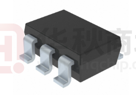
SOT26
AP74700Q supports wide input operation range from 3.2V to 65V,
allowing control of many popular DC rail voltage such as 12V, 24V or
higher automotive battery systems. The 3.2V input voltage support fits
for severe cold crank requirements in automotive systems. The
AP74700Q can withstand and protect the loads from reverse voltages
down to -65V.
VCP
1
6
ANODE
GND
2
5
GATE
EN
3
4
CATHODE
Top View
AP74700Q, with its built-in charge pump, controls the GATE of
MOSFET to regulate the MOSFET’s forward voltage drop to around
20mV. Its internal gate driver quickly turns off the MOSFET during a
reverse current event and ensures there is no DC reverse current
flow. Fast reverse current blocking response of < 0.75µs makes it
suitable for systems with output voltage holdup requirements during
ISO 7637 pulse testing, as well as power fail and input micro-short
conditions.
The high 65V voltage rating of AP74700Q simplifies the system
design for automotive ISO 7637 protection. With the enable pin low,
the controller is off and draws about typical 0.7µA of current.
The AP74700Q is available in SOT26 package.
Features
Applications
Automotive infotainment systems - clusters
Automotive ADAS systems - cameras
Automotive lighting systems
Automotive power trains
Notes:
Input Voltage Ranges from 3.2V to 65V (3.9V Start-up)
-65V Reverse Battery Voltage
Charge Pump for External N-Channel Power MOSFET
20mV ANODE to CATHODE Forward Voltage Drop Control
Low Shutdown Current of 0.7µA when Disabled
Low Quiescent Current of 80µA when Enabled
Fast Reverse Current Block Response Time of < 0.75µs
Active High Enable Operation
ESD Protection 2kV of HBM and 1.5kV of CDM
AEC-Q100 Qualification with Device Temperature Grade 1
(-40°C to +125°C Ambient Operating Temperature Range)
Compliant with Automotive Transient Requirements with
Appropriate TVS
ISO 7637-2 Transient Pulses
ISO 16750-2 Load Dump Suppression
6-Pin SOT26 Package
Totally Lead-Free & Fully RoHS Compliant (Notes 1 & 2)
Halogen and Antimony Free. “Green” Device (Note 3)
The AP74700Q is suitable for automotive applications
requiring specific change control; this part is AEC-Q100
qualified, PPAP capable, and manufactured in IATF16949
certified facilities.
https://www.diodes.com/quality/product-definitions/
1. No purposely added lead. Fully EU Directive 2002/95/EC (RoHS), 2011/65/EU (RoHS 2) & 2015/863/EU (RoHS 3) compliant.
2. See https://www.diodes.com/quality/lead-free/ for more information about Diodes Incorporated’s definitions of Halogen- and Antimony-free, "Green" and
Lead-free.
3. Halogen- and Antimony-free "Green” products are defined as those which contain VCATHODE
0V
VANODE < VCATHODE
-100 mV
tFWD_GATE
VGATE
90%
0V
9 of 21
www.diodes.com
July 2022
© 2022 Copyright Diodes Incorporated. All Rights Reserved.
�AP74700Q
Detailed Description
Overview
The AP74700Q is a ±65V reverse protected ideal diode controller, which can implement an efficient and fast reverse polarity protection circuit or
be used in an ORing configuration. When used with an suitable external N-channel MOSFET it provides a lower loss alternative to other reverse
polarity solutions such as a P-channel MOSFET or a Schottky diode. An internal charge pump is used to drive the external N-channel MOSFET to
a maximum gate drive voltage of approximately 15V. The voltage drop across the MOSFET is continuously monitored between the ANODE and
CATHODE pins, and the GATE to ANODE voltage is adjusted as needed to regulate the forward voltage drop at 20mV. When reverse current
from ANODE to CATHODE is detected, then the MOSFET will be turned off within 0.75µs of fast reverse current response time by internally
connecting GATE to ANODE to avoid DC reverse current flow. An enable pin, EN, when brought low places the AP74700Q into a shutdown mode
which turns off the external N-channel MOSFET and minimizes the AP74700Q’s standby current.
Input Voltage
The ANODE pin is used to power the AP74700Q's internal circuitry, typically drawing 80μA when enabled and 0.7μA when disabled. If the ANODE
pin voltage is greater than the UVLO rising threshold, then AP74700Q operates in either shutdown mode or conduction mode in depending on the
EN pin voltage. The voltage from ANODE to GND is designed to withstand 65V to -65V, allowing the AP74700Q to withstand negative voltage
transients.
Charge Pump
The charge pump supplies the voltage necessary to drive the external N-channel MOSFET. An external charge pump capacitor is placed between
VCP and ANODE pins to provide energy to turn on the external MOSFET. In order for the charge pump to supply current to the external capacitor,
the EN pin voltage must be above the specified input high threshold, VIH_EN. When enabled, the charge pump sources a charging current of
220μA typical. If EN pin is pulled low, then the charge pump remains disabled. To ensure that the external MOSFET can be driven above its
specified threshold voltage, the VCP to ANODE voltage must be above the VCP UVLO, typically 6.6V, before the internal gate driver is enabled.
Initial gate driver enable delay can be calculated with following formula.
𝑇𝐷𝑅𝑉_𝐸𝑁 = 70μs + CVCP 𝑋
VVCP_UVLO
220μA
Where,
CVCP is the charge pump capacitance connected across ANODE and VCP pins
VVCP_UVLO = 6.6V (typical)
Typical 1V hysteresis of VCP UVLO threshold enhances linearity of gate driver. The charge pump remains enabled until the VCP to ANODE
voltage reaches 13V, typically, at which point the charge pump is disabled, decreasing the current draw on the ANODE pin. The charge pump
remains disabled until the VCP to ANODE voltage is below 12V typically, at which point the charge pump is enabled. The voltage between VCP
and ANODE continues to charge and discharge between 12V and 13V. By enabling and disabling the charge pump, the operating quiescent
current of the AP74700Q is reduced. When the charge pump is disabled, it sinks 6μA typical.
Gate Driver
The gate driver controls the external N-channel MOSFET by driving the GATE to ANODE voltage to the corresponding mode of operation. There
are three defined modes of operation that the gate driver operates under forward regulation, full conduction mode and reverse current protection,
according to the ANODE to CATHODE voltage. Its mode varies according to the ANODE to CATHODE voltage of the AP74700Q. The threshold
between forward regulation mode and conduction mode is when the ANODE to CATHODE voltage is 50mV. The threshold between forward
regulation mode and reverse current protection mode is when the ANODE to CATHODE voltage is -10mV.
Reverse Current
Protection Mode
Regulated Conduction Mode
GATE
connected
to ANODE
Document number: DS45004 Rev. 3 - 2
GATE
connected
to VCP
GATE to ANODE Voltage Regulated
-10 mV
AP74700Q
Full Conduction Mode
0V
20 mV
VANODE - VCATHODE
10 of 21
www.diodes.com
50 mV
July 2022
© 2022 Copyright Diodes Incorporated. All Rights Reserved.
�AP74700Q
Detailed Description (continued)
Enable
The EN pin allows for the gate driver to be either enabled or disabled by an external signal. If the EN pin voltage is greater than the rising
threshold, the gate driver and charge pump are activated. If the EN pin voltage is lower than the input low threshold, the charge pump and gate
driver are disabled, placing the AP74700Q in shutdown mode. The EN pin can withstand a voltage as high as 65V and as low as -65V. This allows
for the EN pin to be connected directly to the ANODE pin if enable functionality is not needed. In conditions where EN is left floating, the internal
sink current of 3μA pulls EN pin low and disables the device.
Operations
AP74700Q has shutdown, regulated conduction, full conduction and reverse current protection mode in operation. Details are as follows.
VANODE
-60V to 0V
0V to UVLO
EN
Don’t Care
VCP - VANODE
VANODE - VCATHODE
VCP
VGATE
Reverse Voltage
OFF (No Power)
NA
Don’t Care
< VEN_IL
AP74700Q Mode
Off
Shutdown
Forward Voltage
ANODE
< VCP_UVLO
UVLO to 60V
VCP Charging
< -10mV
ANODE
Reverse Current Protection
-10mV to 50mV
Regulated
Regulated Conduction (Light Load)
> 50mV
VCP
Full Conduction (Heavy Load)
> VEN_IH
On
> VCP_UVLO
Shutdown Mode
The AP74700Q enters shutdown mode when the EN pin voltage is below the specified input low threshold VIL _EN. Both the gate driver and the
charge pump are disabled in shutdown mode. During shutdown mode, the AP74700Q enters low I Q operation with the ANODE pin only sinking
1μA. When the AP74700Q is in shutdown mode, forward current flow through the external MOSFET is not interrupted but is conducted through the
MOSFET's body diode.
Regulated Conduction Mode
For the AP74700Q to operate in regulated conduction mode, the gate driver must be enabled and the current from source to drain of the external
MOSFET must be within the range to result in an ANODE to CATHODE voltage drop of -10mV to 50mV. During forward regulation mode, the
ANODE to CATHODE voltage is regulated to 20mV by adjusting the GATE to ANODE voltage. This regulation enables turning off of the MOSFET
at very light loads and ensures there is no DC reverse current flow.
Full Conduction Mode
For the AP74700Q to operate in full conduction mode, the gate driver must be enabled and the current from source to drain of the external
MOSFET must be large enough to result in an ANODE to CATHODE voltage drop of greater than 50mV typical. If these conditions are achieved,
the GATE pin is internally connected to the VCP pin, resulting in the GATE to ANODE voltage being approximately the same as the VCP to
ANODE voltage. By connecting VCP to GATE, the external MOSFET's RDS(ON) is minimized, reducing the power loss of the external MOSFET
when forward currents are large.
Reverse Current Protection Mode
For the AP74700Q to operate in reverse current protection mode, the gate driver must be enabled and the current of the external MOSFET must
be flowing from the drain to the source. When the ANODE to CATHODE voltage is typically lower than -10mV, reverse current protection mode is
entered, and the GATE pin is internally connected to the ANODE pin and discharges the gate capacitance of the MOSFET turning it off. With the
MOSFET being off, its body diode blocks any reverse current from flowing from the drain to source.
AP74700Q
Document number: DS45004 Rev. 3 - 2
11 of 21
www.diodes.com
July 2022
© 2022 Copyright Diodes Incorporated. All Rights Reserved.
�AP74700Q
Application Information
The AP74700Q is used with N-channel MOSFET in a typical reverse polarity protection application. The schematic for a 12V battery protection
application is shown below where the AP74700Q is used in series with a battery to drive the MOSFET Q1. The TVS is not required for the
AP74700Q to operate, but it is used to clamp the positive and negative voltage surges. The output capacitor COUT is recommended to protect the
immediate output voltage from collapse as a result of line disturbance.
Q1
Battery /
Power
Source
Voltage
Regulator
TVS
CIN
ANODE
EN
GATE
CATHODE
COUT
(DC/DC, LDO)
AP74700Q
C_CP
VCP
GND
Design Example
Design Parameter
VIN Range
VOUT
IOUT
COUT
Automotive EMC
Compliance
Example Value
12V car battery, 12V nominal with 3.2V cold crank and 35V load dump
3.2V during cold crank to 35V load dump
3A nominal and 5A maximum
1μF min, 47μF typical hold-up capacitor
ISO 7637-2 and ISO 16750-2
MOSFET Selection
The important MOSFET electrical parameters are the maximum continuous drain current I D, the maximum drain to source voltage VDS(MAX), the
maximum source current through body diode and the drain-to-source on-resistance RDS(ON).
The maximum continuous drain current, ID, rating must exceed the maximum continuous load current. The maximum drain-to-source voltage,
VDS(MAX), must be high enough to withstand the highest differential voltage seen in the application. This would include any anticipated fault
conditions. It is recommended to use MOSFETs with voltage rating up to 60V maximum with the AP74700Q because anode-cathode maximum
voltage is 65V. The maximum VGS AP74700Q can drive is 13V, so a MOSFET with 15V minimum VGS should be selected.
If a MOSFET with < 15V VGS rating is selected, a Zener diode can be used to clamp VGS to safe level. During startup, inrush current flows through
the body diode to charge the bulk hold-up capacitors at the output. The maximum source current through the body diode must be higher than the
inrush current that can be seen in the application.
To reduce the MOSFET conduction losses, lowest possible RDS(ON) is preferred, but selecting a MOSFET based on low RDS(ON) may not be
beneficial always. Higher RDS(ON) will provide increased voltage information to AP74700Q's reverse comparator at a lower reverse current.
Reverse current detection is better with increased RDS(ON). It is recommended to operate the MOSFET in regulated conduction mode during
nominal load conditions and select RDS(ON) such that at nominal operating current, forward voltage drop V DS is close to 20mV regulation point and
not more than 50mV.
As a guideline, it is suggested to choose (20mV/ILoad(Nominal)) ≤ RDS(ON) ≤ (50mV/ILoad(Nominal)). MOSFET datasheets usually specify RDS(ON) at
4.5V VGS and 10V VGS. RDS(ON) increases drastically below 4.5V VGS and RDS(ON) is highest when VGS is close to MOSFET VTH. For stable
regulation at light load conditions, it is recommended to operate the MOSFET close to 4.5V V GS, that is, much higher than MOSFET gate
threshold voltage. It is recommended to choose MOSFET gate threshold voltage V TH of 2V to 2.5V maximum. Choosing a lower VTH MOSFET
also reduces the turn ON time. Based on the design requirements, preferred MOSFET ratings are:
60V VDS(MAX) and ±20V VGS(MAX)
RDS(ON) at 3A nominal current: (20mV/3A) ≤ RDS(ON) ≤ (50mV/3A) = 6.67mΩ ≤ RDS(ON) ≤ 16.67mΩ.
MOSFET gate threshold voltage VTH: 2V maximum
AP74700Q
Document number: DS45004 Rev. 3 - 2
12 of 21
www.diodes.com
July 2022
© 2022 Copyright Diodes Incorporated. All Rights Reserved.
�AP74700Q
Application Information (continued)
DIODES™ DMT6007LFGQ MOSFET is selected to meet this 12V reverse battery protection design requirements and it is rated at:
60V VDS(MAX) and ±20V VGS(MAX)
RDS(ON) 6.5mΩ typical and 8.5mΩ maximum rated at 4.5V VGS
MOSFET VTH: 2V maximum
Thermal resistance of the MOSFET should be considered against the expected maximum power dissipation in the MOSFET to ensure that the
junction temperature (TJ) is well controlled.
Charge Pump C_CP and CIN/COUT
Minimum required capacitance for charge pump VCP and input/output capacitance are:
C_CP: Minimum 0.1μF is required; recommended value of VCP (μF) ≥ 10 x CISS (MOSFET) (μF)
CIN: Minimum 22nF of input capacitance
COUT: Minimum 1μF of output capacitance.
TVS Selection for 12V Battery Protection Application
TVS diodes are used in automotive systems for protection against transients. In the 12V battery protection application circuit shown below, a
bidirectional TVS diode is used to protect the system from positive and negative transient voltages that occur during normal operation of the car
and these transient voltage levels and pulses are specified in ISO 7637-2 and ISO 16750-2 standards.
There are two important specifications, breakdown voltage and clamping voltage of the TVS. Breakdown voltage is the voltage at which the TVS
diode goes into avalanche similar to a Zener diode and is specified at a low current value typical 1mA, and the breakdown voltage should be
higher than worst case steady state voltages seen in the system. The breakdown voltage of the TVS+ should be higher than 24V jump start
voltage and 35V suppressed load dump voltage and less than the maximum ratings of AP74700Q (65V). The breakdown voltage of TVS- should
be beyond maximum reverse battery voltage -16V, so that the TVS- is not damaged due to long time exposure to reverse connected battery.
Clamping voltage is the voltage the TVS diode clamps in high current pulse situations and this voltage is much higher than the breakdown voltage.
TVS diodes are meant to clamp transient pulses and should not interfere with steady state operation. In the case of ISO 7637-2 Pulse 1, the input
voltage goes up to -150V with a generator impedance of 10Ω. This translates to 15A flowing through the TVS- and the voltage across the TVS
would be close to its clamping voltage.
Q1,
DMT6007LFGQ
12 V
BATTERY
Voltage
Regulator
CIN,
22 nF
ANODE
TVS
TVS
DIODES
DIODES™
SMBJ33CA
SMBJ33CAQ
EN
C_CP,
0.1 uF
GATE
CATHODE
COUT,
47 uF
(DC/DC, LDO)
AP74700Q
VCP
GND
The next criterion is that the absolute maximum rating of ANODE to CATHODE reverse voltage of the AP74700Q (-75V) and the maximum VDS
rating MOSFET are not exceeded. In the design example, 60V rated MOSFET is chosen and maximum limit on the CATHODE to ANODE voltage
is 60V. In case of ISO 7637-2 Pulse 1, the ANODE of AP74700Q is pulled down by the ISO pulse and clamped by TVS-. The MOSFET is turned
off quickly to prevent reverse current from discharging the bulk output capacitors. When the MOSFET turns off, the CATHODE to ANODE voltage
seen is equal to (TVS clamping voltage + output capacitor voltage). If the maximum voltage on output capacitor is 16V (maximum battery voltage),
then the clamping voltage of the TVS- should not exceed, (60V – 16V) = -44V.
The SMBJ33CAQ TVS diode can be used for 12V battery protection application. The breakdown voltage of 36.7V meets the jump start, load dump
requirements on the positive side and 16V reverse battery connection on the negative side. During ISO 7637-2 Pulse 1 test, the SMBJ33CAQ
clamps at -44V with 15A of peak surge current as shown below and it meets the clamping voltage ≤ 44V. SMBJ series of TVS' are rated up to
600W peak pulse power levels. This is sufficient for ISO 7637-2 Pulses and suppressed load dump (ISO-16750-2 Pulse B).
AP74700Q
Document number: DS45004 Rev. 3 - 2
13 of 21
www.diodes.com
July 2022
© 2022 Copyright Diodes Incorporated. All Rights Reserved.
�AP74700Q
Application Information (continued)
TVS Selection for 24V Battery Protection Application
Typical 24V battery protection application circuit shown below uses two unidirectional TVS diodes to protect the system from positive and negative
transient voltages.
Q1,
DMT6007LFGQ
24 V
BATTERY
TVS+
DIODES
SMBJ58AQ
TVSDIODES
SMBJ26AQ
Voltage
Regulator
CIN,
22 nF
ANODE
EN
C_CP,
0.1 uF
GATE
CATHODE
COUT,
47 uF
(DC/DC, LDO)
AP74700Q
VCP
GND
The breakdown voltage of the TVS+ should be higher than 48V jump start voltage, lower than the absolute maximum ratings of ANODE and EN
pins of AP74700Q (65V) and should withstand 65V suppressed load dump. The breakdown voltage of TVS- should be lower than maximum
reverse battery voltage -32V, so that the TVS- is not damaged due to long time exposure to reverse connected battery.
During ISO 7637-2 Pulse 1, the input voltage goes up to -600V with a generator impedance of 50Ω. This translates to 12A flowing through the
TVS-. The clamping voltage of the TVS- cannot be same as that of 12V battery protection circuit. Because during the ISO 7637-2 Pulse, the
ANODE to CATHODE voltage seen is equal to (-TVS clamping voltage + output capacitor voltage). For 24V battery application, the maximum
battery voltage is 32V, then the clamping voltage of the TVS- should not exceed, 75V – 32V = 43V.
Single bidirectional TVS cannot be used for 24V battery protection because breakdown voltage for TVS+ ≥ 65V, maximum clamping voltage is ≤
43V and the clamping voltage cannot be lower than the breakdown voltage. Two unidirectional TVS connected back-back needs to be used at the
input. For positive side TVS+, SMBJ58AQ with the breakdown voltage of 64.4V (minimum), 67.8V (typical) is recommended. For the negative side
TVS-, SMBJ26AQ with breakdown voltage close to 32V (to withstand maximum reverse battery voltage -32V) and maximum clamping voltage of
42.1V is recommended. For 24V battery protection, a 75V rated MOSFET is recommended to be used along with SMBJ26AQ and SMBJ58AQ
connected back-back at the input.
Application Curves
VOUT
VGATE
GATE Turn Off Quickly < 1µs
VIN
IIN
ISO 7637-2 Pulse 1
AP74700Q
Document number: DS45004 Rev. 3 - 2
TVS Clamping at -41V
Response to ISO 7637-2 Pulse 1
14 of 21
www.diodes.com
July 2022
© 2022 Copyright Diodes Incorporated. All Rights Reserved.
�AP74700Q
Application Information (continued)
Start-up with 3A Load
CH1 = VIN, CH2 = VOUT, CH3 = VGATE, CH4 = IIN
Start-up with 6A Load
CH1 = VIN, CH2 = VOUT, CH3 = VGATE, CH4 = IIN
VIN
VIN
VOUT
VOUT
VGATE
VGATE
IIN
IIN
VCP During Start-up with 3A Load
CH1 = VIN, CH2 = VCP, CH3 = VGATE, CH4 = IIN
VCP During Start-up with 5.8A Load
CH1 = VIN, CH2 = VCP, CH3 = VGATE, CH4 = IIN
VIN
VIN
VCP
VCP
VGATE
VGATE
IIN
IIN
ORing VIN1 to VIN2 Switch Over
CH1 = VIN1, CH2 = VOUT, CH3 = VGATE1, CH4 = IIN1
VIN1
ORing VIN1 to VIN2 Switch Over
CH1 = VIN1, CH2 = VOUT, CH3 = VGATE1, CH4 = IIN2
VIN1
VOUT
VOUT
VOUT switches to VIN2 15V
VGATE1
VOUT switches to VIN2 15V
VGATE1
IIN1
IIN2
AP74700Q
Document number: DS45004 Rev. 3 - 2
15 of 21
www.diodes.com
July 2022
© 2022 Copyright Diodes Incorporated. All Rights Reserved.
�AP74700Q
Application Information (continued)
ORing VIN2 to VIN1 Switch Over
CH1 = VIN1, CH2 = VOUT, CH3 = VGATE1, CH4 = IIN1
VIN1
VOUT
ORing VIN2 to VIN1 Switch Over
CH1 = VIN1, CH2 = VOUT, CH3 = VGATE1, CH4 = IIN2
VIN1
VOUT switches to VIN1 12V
VGATE1
VOUT
VOUT switches to VIN1 12V
VGATE1
IIN2
IIN1
ORing VIN2 Failure and Switch Over to VIN1
CH1 = VOUT, CH2 = VIN1, CH3 = VGATE1, CH4 = IIN1
VOUT
ORing VIN2 Failure and Switch Over to VIN1
CH1 = VOUT, CH2 = VIN1, CH3 = VIN2, CH4 = IIN2
VOUT
VIN1
VIN1
VGATE1
VIN2
IIN1
IIN2
ORing Application Implementation
Basic redundant power architecture comprises of two or more voltage or power supply sources driving a single load. In its simplest form, the
ORing solution for redundant power supplies consists of Schottky ORing diodes that protect the system against an input power supply fault
condition. A diode ORing device provides effective and low cost solution with few components. However, the diodes forward voltage drops affect
the efficiency of the system permanently, since each diode in an ORing application spends most of its time in forward conduction mode. These
power losses increase the requirements for thermal management and allocated board space.
The AP74700Q ICs combined with external N-channel MOSFETs can be used in ORing solution. The forward diode drop is reduced as the
external N-channel MOSFET is turned ON during normal operation. AP74700Q quickly detects the reverse current, pulls down the MOSFET gate
fast, leaving the body diode of the MOSFET to block the reverse current flow. An effective ORing solution needs to be extremely fast to limit the
reverse current amount and duration. The AP74700Q devices in ORing configuration constantly sense the voltage difference between ANODE
and CATHODE pins, which are the voltage levels at the power sources (VIN1, VIN2) and the common load point respectively. The source to drain
voltage VDS for each MOSFET is monitored by the ANODE and CATHODE pins of the AP74700Q. A fast comparator shuts down the Gate Driver
through a fast pull-down within 0.45μs (typical) as soon as V(IN) – V(OUT) falls below -10mV. It turns on the Gate Driver with 10mA gate charge
current once the differential forward voltage V(IN) – V(OUT) exceeds 50mV.
AP74700Q
Document number: DS45004 Rev. 3 - 2
16 of 21
www.diodes.com
July 2022
© 2022 Copyright Diodes Incorporated. All Rights Reserved.
�AP74700Q
Application Information (continued)
Q1
TVS
Load
VIN1
CIN
ANODE
EN
GATE
CATHODE
COUT
AP74700Q
C_CP
VCP
GND
Q2
TVS
VIN2
CIN
ANODE
EN
GATE
CATHODE
AP74700Q
C_CP
VCP
GND
AP74700Q
Document number: DS45004 Rev. 3 - 2
17 of 21
www.diodes.com
July 2022
© 2022 Copyright Diodes Incorporated. All Rights Reserved.
�AP74700Q
Ordering Information
AP74700 X XX - X
Grade
Package
Packing
Q : Automotive Grade
W6 : SOT26
7 : Tape & Reel
Part Number
Part Number Suffix
Enable Active
Package Code
Package
AP74700QW6-7
-7
High
W6
SOT26
Packing
Qty.
Carrier
3000
7” Tape and Reel
Marking Information
SOT26
( Top View )
5
4
7
6
XXX
YWX
1
AP74700Q
Document number: DS45004 Rev. 3 - 2
2
3
XXX : Identification Code
Y : Year 0 to 9 (ex: 2 = 2022)
W : Week : A to Z : week 1 to 26;
a to y : week 27 to 51;
z : week 52 and 53
X : Internal Code
Part Number
Package
Identification Code
AP74700QW6-7
SOT26
T8Q
18 of 21
www.diodes.com
July 2022
© 2022 Copyright Diodes Incorporated. All Rights Reserved.
�AP74700Q
Package Outline Dimensions
Please see http://www.diodes.com/package-outlines.html for the latest version.
SOT26
D
E1
SOT26
Dim Min Max
Typ
A1 0.013 0.10
0.05
A2 1.00 1.30
1.10
A3 0.70 0.80
0.75
b
0.35 0.50
0.38
c
0.10 0.20
0.15
D
2.90 3.10
3.00
e
0.95
e1
1.90
E
2.70 3.00
2.80
E1 1.50 1.70
1.60
L
0.35 0.55
0.40
a
8°
a1
7°
All Dimensions in mm
E
b
a1
e1
A2
A3
A1
Seating Plane
e
L
c
a
Suggested Pad Layout
Please see http://www.diodes.com/package-outlines.html for the latest version.
SOT26
C1
Y1
G
C
Dimensions Value (in mm)
C
2.40
C1
0.95
G
1.60
X
0.55
Y
0.80
Y1
3.20
Y
X
Notes:
10. The suggested land pattern dimensions have been provided for reference only, as actual pad layouts may vary depending on application. These
dimensions may be modified based on user equipment capability or fabrication criteria. A more robust pattern may be desired for wave soldering and is
calculated by adding 0.2mm to the ‘Z’ dimension. For further information, please reference document IPC-7351A, Naming Convention for Standard SMT
Land Patterns, and for International grid details, please see document IEC, Publication 97.
11. For high voltage applications, the appropriate industry sector guidelines should be considered with regards to creepage and clearance distances
between device terminals and PCB tracking.
Mechanical Data
Surface Mount Package
Moisture Sensitivity: Level 1 per J-STD-020
Package Material: Molded Plastic, UL Flammability Classification Rating 94V-0
Terminals: Finish – Matte Tin Plated Leads, Solderable per MIL-STD-202, Method 208
Weight: 0.016 grams (Approximate)
Max Soldering Temperature +260°C for 30 secs as per JEDEC J-STD-020
AP74700Q
Document number: DS45004 Rev. 3 - 2
19 of 21
www.diodes.com
July 2022
© 2022 Copyright Diodes Incorporated. All Rights Reserved.
�AP74700Q
Device Taping Orientation
Package Type: SOT26
Tape Width Part Number Suffix
Tape Orientation
-7
-13
TA
TC
8mm
Direction of feed
Notes:
12. For part marking, refer to product datasheet.
13. Tape and package drawings are not to scale and are shown for device tape orientation only.
14. The taping orientation of the other package type can be found on our website at https://www.diodes.com/assets/Packaging-Support-Docs/ap02007.pdf.
AP74700Q
Document number: DS45004 Rev. 3 - 2
20 of 21
www.diodes.com
July 2022
© 2022 Copyright Diodes Incorporated. All Rights Reserved.
�AP74700Q
IMPORTANT NOTICE
1.
DIODES INCORPORATED (Diodes) AND ITS SUBSIDIARIES MAKE NO WARRANTY OF ANY KIND, EXPRESS OR IMPLIED, WITH
REGARDS TO ANY INFORMATION CONTAINED IN THIS DOCUMENT, INCLUDING, BUT NOT LIMITED TO, THE IMPLIED WARRANTIES OF
MERCHANTABILITY, FITNESS FOR A PARTICULAR PURPOSE OR NON-INFRINGEMENT OF THIRD PARTY INTELLECTUAL PROPERTY
RIGHTS (AND THEIR EQUIVALENTS UNDER THE LAWS OF ANY JURISDICTION).
2.
The Information contained herein is for informational purpose only and is provided only to illustrate the operation of Diodes’ products
described herein and application examples. Diodes does not assume any liability arising out of the application or use of this document or any
product described herein. This document is intended for skilled and technically trained engineering customers and users who design with Diodes’
products. Diodes’ products may be used to facilitate safety-related applications; however, in all instances customers and users are responsible for
(a) selecting the appropriate Diodes products for their applications, (b) evaluating the suitability of Diodes’ products for their intended applications,
(c) ensuring their applications, which incorporate Diodes’ products, comply the applicable legal and regulatory requirements as well as safety and
functional-safety related standards, and (d) ensuring they design with appropriate safeguards (including testing, validation, quality control
techniques, redundancy, malfunction prevention, and appropriate treatment for aging degradation) to minimize the risks associated with their
applications.
3.
Diodes assumes no liability for any application-related information, support, assistance or feedback that may be provided by Diodes
from time to time. Any customer or user of this document or products described herein will assume all risks and liabilities associated with such
use, and will hold Diodes and all companies whose products are represented herein or on Diodes’ websites, harmless against all damages and
liabilities.
4.
Products described herein may be covered by one or more United States, international or foreign patents and pending patent
applications. Product names and markings noted herein may also be covered by one or more United States, international or foreign trademarks
and trademark applications. Diodes does not convey any license under any of its intellectual property rights or the rights of any third parties
(including third parties whose products and services may be described in this document or on Diodes’ website) under this document.
5.
Diodes’
products
are
provided
subject
to
Diodes’
Standard
Terms
and
Conditions
of
Sale
(https://www.diodes.com/about/company/terms-and-conditions/terms-and-conditions-of-sales/) or other applicable terms. This document does not
alter or expand the applicable warranties provided by Diodes. Diodes does not warrant or accept any liability whatsoever in respect of any
products purchased through unauthorized sales channel.
6.
Diodes’ products and technology may not be used for or incorporated into any products or systems whose manufacture, use or sale is
prohibited under any applicable laws and regulations. Should customers or users use Diodes’ products in contravention of any applicable laws or
regulations, or for any unintended or unauthorized application, customers and users will (a) be solely responsible for any damages, losses or
penalties arising in connection therewith or as a result thereof, and (b) indemnify and hold Diodes and its representatives and agents harmless
against any and all claims, damages, expenses, and attorney fees arising out of, directly or indirectly, any claim relating to any noncompliance with
the applicable laws and regulations, as well as any unintended or unauthorized application.
7.
While efforts have been made to ensure the information contained in this document is accurate, complete and current, it may contain
technical inaccuracies, omissions and typographical errors. Diodes does not warrant that information contained in this document is error-free and
Diodes is under no obligation to update or otherwise correct this information. Notwithstanding the foregoing, Diodes reserves the right to make
modifications, enhancements, improvements, corrections or other changes without further notice to this document and any product described
herein. This document is written in English but may be translated into multiple languages for reference. Only the English version of this document
is the final and determinative format released by Diodes.
8.
Any unauthorized copying, modification, distribution, transmission, display or other use of this document (or any portion hereof) is
prohibited. Diodes assumes no responsibility for any losses incurred by the customers or users or any third parties arising from any such
unauthorized use.
9.
This Notice may be periodically updated with the most recent version available at https://www.diodes.com/about/company/terms-andconditions/important-notice
DIODES is a trademark of Diodes Incorporated in the United States and other countries.
The Diodes logo is a registered trademark of Diodes Incorporated in the United States and other countries.
© 2022 Diodes Incorporated. All Rights Reserved.
www.diodes.com
AP74700Q
Document number: DS45004 Rev. 3 - 2
21 of 21
www.diodes.com
July 2022
© 2022 Copyright Diodes Incorporated. All Rights Reserved.
�