ATS177
SINGLE OUTPUT HALL EFFECT LATCH
Description
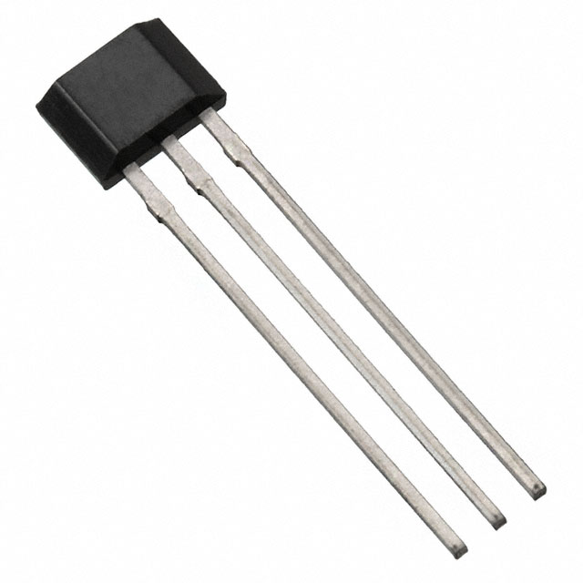
Pin Assignments
ATS177 is an integrated Hall-Effect latch sensor designed for
electronic commutation of brush-less DC motor applications.
The device includes an on-chip Hall voltage generator for
magnetic sensing, a comparator that amplifies the Hall
voltage, and a schmitt trigger to provide switching hysteresis
for noise rejection, and open-collector output. An internal
bandgap regulator provides a temperature compensated
supply voltage for internal circuits and allows a wide operating
supply range.
When the magnetic flux density (B) is larger than operate
point (Bop), output is switched on (DO pin is pulled low). The
output state is held on until a magnetic flux density reversal
falls below Brp. When B is less than Brp, the output is
switched off.
(Top View)
3. DO
2. GND
1. Vcc
SIP-3L
Applications
•
•
•
•
Brush-less DC Motor
Brush-less DC Fan
Revolution counting
Speed measurement
The ATS177 is available in SIP-3L package.
Features
•
•
•
•
•
•
•
•
•
Bipolar Hall-Effect latch sensor
3.5V to 20V DC operating voltage
Temperature compensation
Open-collector pre-driver
25mA maximum output sink current
Built-in reverse polarity protection
Operating temperature: -40°C to +125°C
SIP-3L package
Green Molding Compound (No Br, Sb) (Note 1)
Notes:
1. EU Directive 2002/95/EC (RoHS). All applicable RoHS exemptions applied. Please visit our website at
http://www.diodes.com/products/lead_free.html.
Typical Application Circuit
+12V
D1
L1
R1
2K
L2
U1
R2
1
VCC OUTPUT
GND
2 ATS177
3
Q1
NPN
3K
+
C1
0.47uF
Q2
NPN
+
C2
0.47uF
Brush-less DC Fan
ATS177
Document number: DS31055 Rev. 6 - 2
1 of 9
www.diodes.com
July 2010
© Diodes Incorporated
�ATS177
SINGLE OUTPUT HALL EFFECT LATCH
Pin Descriptions
Pin name
P/I/O
Pin #
Vcc
GND
DO
P
P
O
1
2
3
Description
Positive power supply
Ground
Digital output
Functional Block Diagram
Vcc
1
Regulator
Hall
plate
23 DO
Amp
2
GND
Absolute Maximum Ratings (TA = 25°C)
Symbol
VCC
VRCC
B
VCE
PD
IC
TJ(MAX)
TS
Characteristics
Supply Voltage
Reverse VCC Polarity Voltage
Magnetic Flux Density
Output OFF Voltage
Package Power Dissipation
Output “ON” Current
Maximum Junction Temperature
Storage Temperature Range
SIP-3L
Continuous
Rating
20
-20
Unlimited
30
550
25
150
-65~+150
Unit
V
V
V
mW
mA
°C
°C
Recommended Operating Conditions
Symbol
VCC
TA
Notes:
Characteristic
Supply Voltage
Operating Ambient Temperature
(Note 2)
Conditions
Min
Max
Unit
Operating
3.5
20
V
Operating
-20
85
°C
2. Shall not exceed PD and Safety Operation Area.
ATS177
Document number: DS31055 Rev. 6 - 2
2 of 9
www.diodes.com
July 2010
© Diodes Incorporated
�ATS177
SINGLE OUTPUT HALL EFFECT LATCH
Electrical Characteristics (TA = 25°C)
Symbol
VCE (sat)
Icex
Icc
tr
tf
Characteristic
Output Saturation Voltage
Output Leakage Current
Supply Current
Output Rise Time
Output Falling Time
Test Conditions
VCC = 14V, Ic = 20mA
VCE = 14V, VCC = 14V
VCC = 20V, Output Open
VCC = 14V, RL = 820Ω, CL = 20pF
VCC = 14V, RL = 820Ω, CL = 20pF
Min
-
Typ.
300
很抱歉,暂时无法提供与“ATS177-PG-B-A”相匹配的价格&库存,您可以联系我们找货
免费人工找货