AZ39151
1.5A ULTRA LOW DROPOUT LINEAR REGULATOR
Description
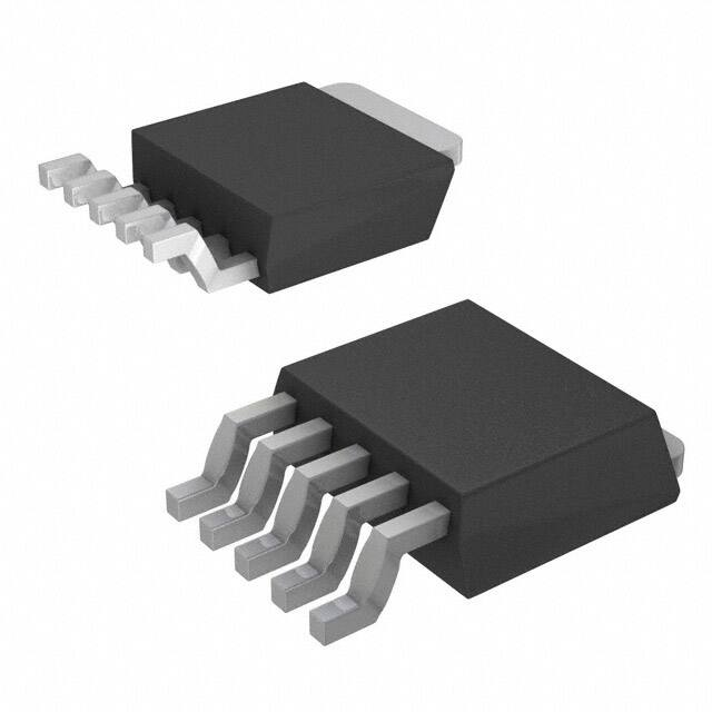
Pin Assignments
The AZ39151 is a 1.5A, high accuracy linear voltage regulator. It
features 375mV dropout voltage at 1.5A output current and low
ground current over all operating conditions.
(Top View)
The AZ39151 is specifically designed for low voltage, high current
output systems, such as PC add-in cards where their tiny dropout
voltage and ground current values are important attributes.
The AZ39151 has fixed 3.3V, 5.0V versions and ADJ (1.25V) version.
5
NC/ADJ
4
VOUT
3
GND
2
VIN
1
EN
The AZ39151 is available in TO-252-5 package.
TO-252-5
Features
Applications
Minimum Guaranteed Output Current: 1.5A
Low Dropout Voltage: 375mV at IOUT = 1.5A
Output Accuracy: ±1%
Low Ground Current
Internal Current and Thermal Limit
Reversed-battery and Reversed-lead Insertion Protection
Fast Transient Response
TTL/CMOS Compatible Enable Pin
Set-top Box
Hi-end DVD Player/Recorder
LCD TV/PDP
LDO Linear Regulator for PC Add-in Cards
High Efficiency Linear Power Supplies
SMPS Post Regulator
Typical Applications Circuit
2
VIN
VEN
CIN
1
+
VIN
EN
VOUT
AZ39151
NC
4
VOUT
5
+ C
OUT
F
GND
F
3
Fixed Version
2
VIN
VEN
CIN
+
F
1
VIN
EN
VOUT
AZ39151
4
VOUT
R1
ADJ
GND
3
5
R2
+ C
OUT
F
VOUT = 1.25*(1+R1/R2)V
Adjustable Version
AZ39151
Document number: DS41513 Rev. 2 - 2
1 of 10
www.diodes.com
October 2018
© Diodes Incorporated
�AZ39151
Pin Description
Pin Number
Pin Name
Function
1
EN
Enable: TTL/CMOS compatible input. Logic high=enable;
Logic low or open=shutdown
2
VIN
Unregulated input
3
GND
Ground pin. This pin and TAB are internally connected
4
VOUT
Regulated output
5
NC/ADJ
No Connection / Adjustable Output
Functional Block Diagram
Fixed Version
AZ39151
Document number: DS41513 Rev. 2 - 2
2 of 10
www.diodes.com
October 2018
© Diodes Incorporated
�AZ39151
Functional Block Diagram (Cont.)
Adjustable Version
Absolute Maximum Ratings (Note 1)
Symbol
Rating
Unit
VIN
Input Voltage
15
V
VEN
Enable Voltage
15
V
+150
°C
-65 to +150
°C
TJ
Operating Junction Temperature
TSTG
Storage Temperature Range
TLEAD
Lead Temperature (Soldering, 10sec)
+260
°C
ESD
ESD (Human Body Model)
5000
V
ESD
ESD (Machine Model)
450
V
Thermal Resistance
100
°C/W
JA
Note:
Parameter
1. Stresses greater than those listed under “Absolute Maximum Ratings” may cause permanent damage to the device. These are stress ratings only, and
functional operation of the device at these or any other conditions beyond those indicated under “Recommended Operating Conditions” is not implied.
Exposure to “Absolute Maximum Ratings” for extended periods may affect device reliability.
Recommended Operating Conditions
Symbol
Parameter
Min
Max
Unit
VIN
Input Voltage
—
13.5
V
VEN
Enable Voltage
—
13.5
V
Operating Junction Temperature
-40
+125
°C
TJ
AZ39151
Document number: DS41513 Rev. 2 - 2
3 of 10
www.diodes.com
October 2018
© Diodes Incorporated
�AZ39151
Electrical Characteristics
(Operating Conditions: VIN = VOUT + 1V, IOUT = 10mA, CIN = 10µF, COUT = 10µF, TJ = +25°C, unless
otherwise specified. The Boldface applies over -40°C ≤ TJ ≤ +125°C.)
Symbol
VOUT
Parameter
Output Voltage
Conditions
Min
Typ
Max
—
-1
—
1
10mA ≤ IOUT ≤ 1.5A,
VOUT + 1V ≤ VIN ≤ 13.5V
-2
—
2
Unit
%
VRLINE
Line Regulation
VOUT + 1V ≤ VIN ≤ 13.5V
—
3
25
mV
VRLOAD
Load Regulation
10mA ≤ IOUT ≤ 1.5A
—
10
50
mV
Output Voltage
Temperature Coefficient
(Note 2)
—
—
100
500
µV/°C
—
—
20
100
ppm/°C
IOUT = 100mA
—
80
200
mV
IOUT = 750mA
—
260
—
mV
IOUT = 1.5A
—
375
700
mV
IOUT = 750mA
—
5
10
mA
IOUT = 1.5A
—
17
34
mA
Standby Current
VIN = 13.5V, VEN = 0V
—
130
220
µA
Dropout Ground Pin Current
VIN ≤ VOUT(NOMINAL) - 0.5V
—
5
—
mA
Short Circuit Current
VOUT = 0V
—
2.8
—
A
Output Noise Voltage (rms)
10Hz to 100kHz, IOUT = 100mA
—
200
—
µV
Minimum Load Current
—
—
—
5
mA
Power Supply Ripple Rejection
f = 120Hz, IOUT = 750mA
49
65
—
dB
Logic low (off)
—
—
0.8
Logic high (on)
2.25
—
—
VEN = VIN
—
15
35
VEN = 0.8V
—
—
4
VEN ≤ 0.8V, VIN ≤ 8V,
VOUT = 0V
—
5
10
ΔVOUT/ΔT
(ΔVOUT/VOUT)ΔT
VDROP
IGND
ISTD
IGND(DO)
ISHORT
—
ILOAD (MIN)
PSRR
Dropout Voltage (Note 3)
ΔVOUT = 1%
Ground Current
Enable Input
VEN
IEN
IOUT (SHDN)
Notes:
Enable Voltage
V
Enable Current
Shutdown Output Current
µA
µA
2. Output voltage temperature coefficient is defined as the worst case voltage change divided by the total temperature range.
3. Dropout voltage is defined as the input-to-output differential when the output voltage drops to 99% of its nominal value which is measured at VOUT + 1V
applied to VIN.
AZ39151
Document number: DS41513 Rev. 2 - 2
4 of 10
www.diodes.com
October 2018
© Diodes Incorporated
�AZ39151
Performance Characteristics
Dropout Voltage vs. Output Current
Dropout Voltage vs. Junction Temperature
500
700
450
650
600
550
Dropout Voltage (mV)
Dropout Voltage (mV)
400
350
300
250
200
150
VIN=6V
100
500
450
400
350
300
250
VOUT=VOUT(NOMINAL)x99%
IOUT=1.5A
o
TJ=25 C
200
50
150
0
100
0
250
500
750
1000
1250
1500
-25
0
25
50
75
100
125
o
Junction Temperature ( C)
Output Current (mA)
Output Voltage vs. Input Voltage
Ground Current vs. Input Voltage
5.5
45
5.0
VEN=3.3V
40
o
TJ=25 C
4.5
35
Ground Current (mA)
Output Voltage (V)
4.0
3.5
10mA
1500mA
3.0
2.5
2.0
1.5
VEN=2.5V
1.0
TJ=25 C
30
IOUT=10mA
IOUT=750mA
IOUT=1500mA
25
20
15
10
o
5
0.5
0.0
0
0
2
4
6
8
10
12
0
2
4
6
Ground Current vs. Output Current
10
27
2.50
24
2.25
21
2.00
18
1.75
15
12
9
6
VIN=6V
3
1.50
1.25
1.00
0.75
VIN=VEN=6V
IOUT=10mA
0.50
o
TJ=25 C
0.25
0
-3
0
200
400
600
800
1000
1200
1400
0.00
-40
Document number: DS41513 Rev. 2 - 2
-20
0
20
40
60
80
100
120
o
Junction Temperature ( C)
Output Current (mA)
AZ39151
12
Ground Current vs. Junction Temperature
Ground Current (mA)
Ground Current (mA)
8
Input Voltage (V)
Input Voltage (V)
5 of 10
www.diodes.com
October 2018
© Diodes Incorporated
�AZ39151
Performance Characteristics (Cont.)
Ground Current vs. Junction Temperature
Ground Current vs. Junction Temperature
25
11
VIN=VEN=6V
IOUT=750mA
VIN=VEN=6V
IOUT=1.5A
24
Ground Current (mA)
Ground Current (mA)
10
9
8
7
6
23
22
21
20
19
5
-40
-20
0
20
40
60
80
100
18
-40
120
-20
0
40
60
80
Junction Temperature ( C)
Short Circuit Current vs. Junction Temperature
Output Voltage vs. Junction Temperature
4.5
5.010
4.0
5.005
3.5
5.000
3.0
2.5
2.0
4.990
4.985
4.980
1.5
VIN=VEN=6V
IOUT=10mA
4.975
1.0
4.970
0.5
-25
0
25
50
75
100
-25
125
0
25
50
75
100
125
o
o
Junction Temperature ( C)
Junction Temperature ( C)
Enable Current vs. Junction Temperature
Line Transient
(Conditions: VIN = 5 to 7V, IOUT = 1.5A, COUT = 10µF)
20
4
ΔVIN (2V/Div)
18
16
14
12
ΔVOUT (100mV/Div)
10
8
6
VIN=VEN=6V
IOUT=10mA
4
2
2
0
-2
100
0
-100
-200
0
-25
0
25
50
75
100
125
Time (10µs/Div)
o
AZ39151
120
4.995
VIN=VEN=6V
Enable Current (A)
100
Junction Temperature ( C)
Output Voltage (V)
Short Circuit Current (A)
20
o
o
Junction Temperature ( C)
Document number: DS41513 Rev. 2 - 2
6 of 10
www.diodes.com
October 2018
© Diodes Incorporated
�AZ39151
Performance Characteristics (Cont.)
Load Transient
(Conditions: VIN = 6V, IOUT = 10mA to 1.5A,
CIN = COUT = 10µF)
PSRR vs. Frequency
(Conditions: VIN = 6V, IOUT = 10mA,
CIN = COUT = 10µF)
80
IOUT (1A/Div)
1
70
0.5
60
0
50
PSRR (dB)
ΔVOUT (0.5V/Div)
1.5
2
40
30
1
20
0
10
-1
0
10
Time (200µs/Div)
100
1k
10k
100k
Frequency (Hz)
AZ39151
Document number: DS41513 Rev. 2 - 2
7 of 10
www.diodes.com
October 2018
© Diodes Incorporated
�AZ39151
Ordering Information
AZ39151 X - X X X
Product Name
Package
TO-252-5
Package
Output Voltage
Packing
E1/G1
D5 : TO-252-5
3.3 : Fixed Output 3.3V
5.0 : Fixed Output 5.0V
ADJ : ADJ Output
TR : Tape & Reel
Blank : Tube
E1 : RoHS Compliant
G1 : RoHS Compliant
and Green
Temperature
Range
-40 to +125°C
AZ39151
Document number: DS41513 Rev. 2 - 2
Part Number
Marking ID
Packing
RoHS Compliant
and Green
RoHS Compliant
RoHS Compliant
and Green
AZ39151D5-3.3E1
AZ39151D53.3G1
AZ39151D5-3.3E1
AZ39151D53.3G1
Tube
AZ39151D53.3TRE1
AZ39151D53.3TRG1
AZ39151D5-3.3E1
AZ39151D53.3G1
Tape & Reel
AZ39151D5-5.0E1
AZ39151D55.0G1
AZ39151D5-5.0E1
AZ39151D55.0G1
Tube
AZ39151D55.0TRE1
AZ39151D55.0TRG1
AZ39151D5-5.0E1
AZ39151D55.0G1
Tape & Reel
AZ39151D5-ADJE1
AZ39151D5ADJG1
AZ39151D5ADJE1
AZ39151D5ADJG1
Tube
AZ39151D5ADJTRE1
AZ39151D5ADJTRG1
AZ39151D5ADJE1
AZ39151D5ADJG1
Tape & Reel
RoHS Compliant
8 of 10
www.diodes.com
October 2018
© Diodes Incorporated
�AZ39151
Package Outline Dimensions (All dimensions in mm(inch).)
(1)
Package Type: TO-252-5
6.350(0.250)
6.650(0.262)
5.200(0.205)
5.400(0.213)
9.500(0.374)
9.900(0.390)
2.200(0.087)
2.400(0.094)
0.430(0.017)
0.580(0.023)
5.400(0.213)
5.700(0.224)
3.800(0.150)
REF
0.000(0.000)
0.127(0.005)
2.550(0.100)
2.900(0.114)
1.270(0.050)
TYP
2.540(0.100)
TYP
0.400(0.016)
0.600(0.024)
0.430(0.017)
0.580(0.023)
1.400(0.055)
1.780(0.070)
AZ39151
Document number: DS41513 Rev. 2 - 2
9 of 10
www.diodes.com
October 2018
© Diodes Incorporated
�AZ39151
IMPORTANT NOTICE
DIODES INCORPORATED MAKES NO WARRANTY OF ANY KIND, EXPRESS OR IMPLIED, WITH REGARDS TO THIS DOCUMENT,
INCLUDING, BUT NOT LIMITED TO, THE IMPLIED WARRANTIES OF MERCHANTABILITY AND FITNESS FOR A PARTICULAR PURPOSE
(AND THEIR EQUIVALENTS UNDER THE LAWS OF ANY JURISDICTION).
Diodes Incorporated and its subsidiaries reserve the right to make modifications, enhancements, improvements, corrections or other changes
without further notice to this document and any product described herein. Diodes Incorporated does not assume any liability arising out of the
application or use of this document or any product described herein; neither does Diodes Incorporated convey any license under its patent or
trademark rights, nor the rights of others. Any Customer or user of this document or products described herein in such applications shall assume
all risks of such use and will agree to hold Diodes Incorporated and all the companies whose products are represented on Diodes Incorporated
website, harmless against all damages.
Diodes Incorporated does not warrant or accept any liability whatsoever in respect of any products purchased through unauthorized sales channel.
Should Customers purchase or use Diodes Incorporated products for any unintended or unauthorized application, Customers shall indemnify and
hold Diodes Incorporated and its representatives harmless against all claims, damages, expenses, and attorney fees arising out of, directly or
indirectly, any claim of personal injury or death associated with such unintended or unauthorized application.
Products described herein may be covered by one or more United States, international or foreign patents pending. Product names and markings
noted herein may also be covered by one or more United States, international or foreign trademarks.
This document is written in English but may be translated into multiple languages for reference. Only the English version of this document is the
final and determinative format released by Diodes Incorporated.
LIFE SUPPORT
Diodes Incorporated products are specifically not authorized for use as critical components in life support devices or systems without the express
written approval of the Chief Executive Officer of Diodes Incorporated. As used herein:
A. Life support devices or systems are devices or systems which:
1. are intended to implant into the body, or
2. support or sustain life and whose failure to perform when properly used in accordance with instructions for use provided in the
labeling can be reasonably expected to result in significant injury to the user.
B. A critical component is any component in a life support device or system whose failure to perform can be reasonably expected to cause the
failure of the life support device or to affect its safety or effectiveness.
Customers represent that they have all necessary expertise in the safety and regulatory ramifications of their life support devices or systems, and
acknowledge and agree that they are solely responsible for all legal, regulatory and safety-related requirements concerning their products and any
use of Diodes Incorporated products in such safety-critical, life support devices or systems, notwithstanding any devices- or systems-related
information or support that may be provided by Diodes Incorporated. Further, Customers must fully indemnify Diodes Incorporated and its
representatives against any damages arising out of the use of Diodes Incorporated products in such safety-critical, life support devices or systems.
Copyright © 2018, Diodes Incorporated
www.diodes.com
AZ39151
Document number: DS41513 Rev. 2 - 2
10 of 10
www.diodes.com
October 2018
© Diodes Incorporated
�