Pb
AZ7500B
BB
PULSE-WIDTH-MODULATION CONTROL CIRCUITS
Lead-Free
Description
Pin Assignments
The AZ7500B is a voltage mode pulse width modulation switching
regulator control circuit designed primarily for power supply control.
(Top View)
The AZ7500B consists of a reference voltage circuit, two error
amplifiers, an on-chip adjustable oscillator, a dead-time control (DTC)
comparator, a pulse-steering control flip-flop, and an output control
circuit. The precision of voltage reference (VREF) is improved up to
±1% through trimming and this provides a better output voltage
regulation. The AZ7500B provides for push-pull or single-ended
output operation, which can be selected through the output control.
1IN+
1
16
2IN+
1IN-
2
15
2IN+
3
14
REF
DTC
4
13
CT
5
12
VCC
RT
6
11
C2
GND
7
10
E2
C1
8
9
E1
FEEDBACK
The difference between AZ7500B and AZ7500C is that they have
4.95V and 5V reference voltage respectively.
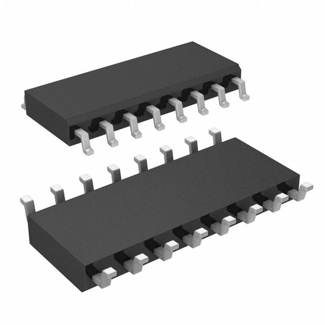
The AZ7500B is available in standard packages of SO-16.
OUTPUT CTRL
Features
SO-16
Stable 4.95V Reference Voltage Trimmed to ±1.0% Accuracy
Uncommitted Output TR for 200mA Sink or Source Current
Single-End or Push-Pull Operation Selected by Output Control
Internal Circuitry Prohibits Double Pulse at Either Output
Complete PWM Control Circuit with Variable Duty Cycle
On-Chip Oscillator with Master or Slave Operation
Totally Lead-Free; RoHS Compliant (Notes 1 & 2)
Notes:
Applications
SMPS
Back Light Inverter
Charger
1. No purposely added lead. Fully EU Directive 2002/95/EC (RoHS) & 2011/65/EU (RoHS 2) compliant.
2. See http://www.diodes.com/quality/lead_free.html for more information about Diodes Incorporated’s definitions of Halogen- and Antimony-free, "Green"
and Lead-free.
Typical Applications Circuit
(VI=10V to 40V)
1mH
2A
KSA1010
(VO=5V, IO=1A)
VO
VI(+)
47
12
11
VCC
3
8
C2
1M
0.1
150
FEED
BACK
C1
5.1k
2
1IN-
14
+
REF
2IN+ 50
50V
AZ7500B
1IN+
2IN+
DTC GND
4
7
E1
9
OUTPUT
CTRL
13
E2
10
RT
6
47k
15
5.1k
5.1k
1
16
CT
150
5
+
50
10V
50 +
10V
0.001
GND
0.1
VI(-)
Pulse Width Modulated Step-down Converter
AZ7500B
Document number: DS38112 Rev. 2 - 2
1 of 10
www.diodes.com
July 2015
© Diodes Incorporated
�AZ7500B
BB
Output Function Table
Signal for Output Control
Output Function
VI = GND
Single-ended or parallel output
VI = VREF
Normal push-pull operation
Functional Block Diagram
OUTPUT CTRL
RT
CT
6
5
13
Oscillator
Pulse-Steering
Flip-Flop
8
Q1
Dead-Time Control
Comparator
DTC
9
D
4
+
Error Amplifier 1
1IN +
1IN -
1
+
11
CK
0.12V
10
PWM
Comparator
FEEDBACK
E2
2
12
2IN -
E1
C2
Q2
+
Error Amplifier 2
2IN +
C1
16
Reference
Regulator
+
15
0.7mA
14
7
VCC
REF
GND
3
AZ7500B
Document number: DS38112 Rev. 2 - 2
2 of 10
www.diodes.com
July 2015
© Diodes Incorporated
�AZ7500B
BB
Absolute Maximum Ratings (Note 3)
Parameter
Symbol
Rating
Unit
VCC
Supply Voltage (Note 4)
40
V
VI
Amplifier Input Voltage
-0.3 to VCC + 0.3
V
VO
Collector Output Voltage
40
V
IO
Collector Output Current
250
mA
Package Thermal Impedance (Note 5)
73
C/W
RθJA
+260
C
TSTG
Storage Temperature Range
-65 to +150
C
–
ESD Rating (Machine Model)
200
V
–
Lead Temperature 1.6mm from case for 10 seconds
Notes: 3. Stresses greater than those listed under “Absolute Maximum Ratings” may cause permanent damage to the device. These are stress ratings only, and
functional operation of the device at these or any other conditions beyond those indicated under “Recommended Operating Conditions” is not implied.
Exposure to “Absolute Maximum Ratings” for extended periods may affect device reliability.
4. All voltage values are with respect to the network ground terminal.
5. Maximum power dissipation is a function of TJ(max), RθJA and TA. The maximum allowable power dissipation at any allowable ambient temperature is P D=
(TJ(max) - TA)/RθJA. Operating at the absolute maximum TJ of +150oC can affect reliability.
Recommended Operating Conditions
Symbol
Parameter
Min
Typ
Max
Unit
Supply Voltage
7
15
36
V
VC1, VC2
Collector Output Voltage
–
30
36
V
IC1, IC2
Collector Output Current
(Each Transistor)
–
–
200
mA
0.3
–
VCC-2
V
VCC
VI
Amplifier Input Voltage
IFB
Current Into Feedback Terminal
–
–
0.3
mA
IREF
Reference Output Current
–
–
10
mA
CT
Timing Capacitor
0.00047
0.001
10
µF
RT
Timing Resistor
1.8
30
500
kΩ
fOSC
Oscillator Frequency
1.0
40
200
kHz
–
PWM Input Voltage (Pin 3, 4, 14)
0.3
–
5.3
V
TA
Operating Free-Air Temperature
-40
–
+85
C
AZ7500B
Document number: DS38112 Rev. 2 - 2
3 of 10
www.diodes.com
July 2015
© Diodes Incorporated
�AZ7500B
BB
Electrical Characteristics
(@VCC=20V, TA= +25C, f=10kHz, unless otherwise specified.)
Parameters
Symbol
Conditions
Min
Typ
Max
Unit
4.90
4.95
5.0
V
4.85
4.95
5.05
V
2
25
mV
Reference Section
VREF
Output Reference Voltage
IREF=1mA
o
IREF=1mA, TA= -40 to +85 C
RLINE
Line Regulation
VCC = 7V to 36V
–
RLOAD
Load Regulation
IREF=1mA to 10mA
–
1
15
mV
Short-Circuit Output Current
VREF = 0V
10
35
50
mA
CT=0.001µF, RT=30KΩ
–
40
–
CT=0.01µF, RT=12KΩ
9.2
10
10.8
9.0
–
12
–
–
1
%
ISC
Oscillator Section
fOSC
Δf /ΔT
Oscillator Frequency
Frequency Change with Temperature
CT=0.01µF, RT=12KΩ,
TA= -40 to +85oC
CT=0.01µF, RT=12KΩ,
TA= -40 to +85oC
kHz
Dead-Time Control Section
Input Bias Current
VCC=15V, V4= 0 to 5.25V
–
-2
-10
µA
Maximum Duty Cycle
VCC=15V, V4= 0V,
Pin 13= VREF
45
–
–
%
Zero Duty Cycle
–
3
3.3
Maximum Duty Cycle
0
–
–
V3 = 2.5V
–
2
10
mV
Input Offset Current
V3 = 2.5V
–
25
250
nA
IBIAS
Input Bias Current
V3 = 2.5V
–
0.2
1
µA
VCM
Common-Mode Input Voltage Range
VCC=7V to 36V
-0.3
–
VCC-2
V
95
–
dB
650
–
kHz
IBIAS
D(MAX)
VITH
Input Threshold Voltage
V
Error-Amplifier Section
VIO
IIO
Input Offset Voltage
GVO
Open-Loop Voltage Gain
VO =0.5V to 3.5V
70
BW
Unity-Gain Bandwidth
–
–
Common-Mode Rejection Ratio
–
65
80
–
dB
Output Sink Current (Feedback)
VID = -15mV to -5V, V3 = 0.7V
-0.3
-0.7
–
mA
Output Source Current (Feedback)
VID=15mV to 5V, V3 = 3.5V
2
–
–
mA
–
4
4.5
V
-0.3
-0.7
–
mA
CMRR
ISINK
ISOURCE
PWM Comparator Section
VITH
Input Threshold Voltage
Zero duty cycle
ISINK
Input Sink Current
V3 = 0.7V
Output Section
VCE(SAT)
VCC(SAT)
IC (OFF)
IE(OFF)
Common Emitter
VE = 0V, IC =200mA
–
1.1
1.3
Emitter Follower
VCC = 15V,
IE = -200mA
–
1.5
2.5
VCE = 36V, VCC=36V
–
2
100
µA
Emitter Off-State Current
VCC = VC = 36V, VE = 0
–
–
-100
µA
Supply Current
Pin 6 = VREF, VCC=15V
–
6
10
mA
Common Emitter
Common Collector
Common Emitter
Common Collector
–
100
200
ns
–
25
100
ns
Output Saturation
Voltage
Collector Off-State Current
V
Total Device
ICC
Output Switching Characteristics
tR
Rise Time
tF
Fall Time
AZ7500B
Document number: DS38112 Rev. 2 - 2
4 of 10
www.diodes.com
July 2015
© Diodes Incorporated
�AZ7500B
BB
Parameter Measurement Information
VCC = 20V
12
4
Test
Inputs
3
12K 6
5
VCC
DTC
C1
FEEDBACK
E1
RT
C2
CT
E2
8
150
4W
150
4W
Output 1
9
11
Output 2
10
0.01F 1
1IN+
2
16
15
13
1IN2IN+
2INOUTPUT
CTRL
GND
REF
14
50K
7
Test Circuit
Voltage
at C1
VCC
Voltage
at C2
VCC
0V
0V
Voltage
at CT
Threshold Voltage
DTC
0V
Threshold Voltage
FEEDBACK
0.7V
Duty Cycle
0%
0%
MAX
Voltage Waveforms
Figure 1. Operational Test Circuit and Waveforms
AZ7500B
Document number: DS38112 Rev. 2 - 2
5 of 10
www.diodes.com
July 2015
© Diodes Incorporated
�AZ7500B
BB
Parameter Measurement Information (Cont.)
+
Amplifier Under Test
VI
FEEDBACK
+
VREF
Other Amplifier
Figure 2. Error Amplifier Characteristics
20V
68
4W
Each Output
Circuit
tF
Output
tR
90%
CL = 15pF
(See Note A)
90%
10%
10%
Note A: CL includes probe and jig capacitance.
Figure 3. Common-Emitter Configuration
20V
Each Output
Circuit
90%
90%
Output
CL = 15pF
(See Note A)
68
4W
10%
10%
tR
tF
Note A: CL includes probe and jig capacitance.
Figure 4. Emitter-Follower Configuration
AZ7500B
Document number: DS38112 Rev. 2 - 2
6 of 10
www.diodes.com
July 2015
© Diodes Incorporated
�AZ7500B
BB
Performance Characteristics
Oscillator Frequency vs. RT and CT
Error Amplifier Small-Signal Voltage Gain vs. Frequency
100
VCC=20V
VCC=20V
VO=3V
90
O
TA=25 C
80
Voltage Gain (dB)
f - Oscillator Frequency (Hz)
100k
0.001F
10k
0.01F
0.1F
o
TA=25 C
70
60
50
40
30
20
10
1k
1k
10k
100k
0
1M
1
RT - Timing Resistance ()
10
100
1k
10k
100k
1M
Frequency (Hz)
Ordering Information
AZ7500B X XX - XX
Product Name
Package
Package
Packing
E1
M: SO-16
TR: Tape & Reel
E1: RoHS Compliant
Temperature Range
SO-16
o
-40 to +85 C
Part Number
AZ7500BMTR-E1
Marking ID
AZ7500BM-E1
Packing
4000/Tape and Reel
Marking Information
(Top View)
First Line: Logo and Marking ID
(See Ordering Information)
Second Line: Date Code
Y: Year
WW: Work Week of Molding
A: Assembly House Code
th
th
XX: 7 and 8 Digits of Batch No.
AZ7500BM-E1
YWWAXX
AZ7500B
Document number: DS38112 Rev. 2 - 2
7 of 10
www.diodes.com
July 2015
© Diodes Incorporated
�AZ7500B
BB
Package Outline Dimensions (All dimensions in mm(inch).)
(1)
Package Type: SO-16
D
D1
7°
0.310(0. 012)
0.510(0. 020)
7°
B
A
20:1
0.250(0.010)
0.400(0. 016)
1.270(0.050)
BSC
9.800(0.386)
10.200(0.402)
1.270(0. 050)
0°
8°
R 0.070(0. 003)
0.200(0. 008)
R 0.070(0. 003)
0.200(0. 008)
B
20:1
8°
C
3°
7°
0.200(0. 008)
Sφ1.000(0. 039)
Depth 0.200(0.008)
8°
A
0.150(0.006)
×45 °
0.400(0.016)
8°
C-C
50:1
1.000(0.039)
0.170(0.007)
0.250(0.010)
3.800(0. 150)
4.040(0. 159)
9.5
°
0.200(0.008)
0.250(0.010)
0.050(0.002)
0.250(0.010)
5.800(0. 228)
6.240(0. 246)
C
Note: Eject hole, oriented hole and mold mark is optional.
D
Symbol
D1
min(mm) max(mm) min(inch) max(inch) min(mm) max(mm) min(inch) max(inch)
Option1
1.350
Option2
AZ7500B
Document number: DS38112 Rev. 2 - 2
-
1.750
1.260
0.053
-
0.069
0.050
1.250
.
1.020
8 of 10
www.diodes.com
1.650
0.049
0.065
-
0.040
-
July 2015
© Diodes Incorporated
�AZ7500B
BB
Suggested Pad Layout
(1)
Package Type: SO-16
Z
G
Y
X
Dimensions
Value
AZ7500B
Document number: DS38112 Rev. 2 - 2
Z
(mm)/(inch)
6.900/0.272
E
G
(mm)/(inch)
3.900/0.154
X
(mm)/(inch)
0.650/0.026
9 of 10
www.diodes.com
Y
(mm)/(inch)
1.500/0.059
E
(mm)/(inch)
1.270/0.050
July 2015
© Diodes Incorporated
�AZ7500B
BB
IMPORTANT NOTICE
DIODES INCORPORATED MAKES NO WARRANTY OF ANY KIND, EXPRESS OR IMPLIED, WITH REGARDS TO THIS DOCUMENT,
INCLUDING, BUT NOT LIMITED TO, THE IMPLIED WARRANTIES OF MERCHANTABILITY AND FITNESS FOR A PARTICULAR PURPOSE
(AND THEIR EQUIVALENTS UNDER THE LAWS OF ANY JURISDICTION).
Diodes Incorporated and its subsidiaries reserve the right to make modifications, enhancements, improvements, corrections or other changes
without further notice to this document and any product described herein. Diodes Incorporated does not assume any liability arising out of the
application or use of this document or any product described herein; neither does Diodes Incorporated convey any license under its patent or
trademark rights, nor the rights of others. Any Customer or user of this document or products described herein in such applications shall assume
all risks of such use and will agree to hold Diodes Incorporated and all the companies whose products are represented on Diodes Incorporated
website, harmless against all damages.
Diodes Incorporated does not warrant or accept any liability whatsoever in respect of any products purchased through unauthorized sales channel.
Should Customers purchase or use Diodes Incorporated products for any unintended or unauthorized application, Customers shall indemnify and
hold Diodes Incorporated and its representatives harmless against all claims, damages, expenses, and attorney fees arising out of, directly or
indirectly, any claim of personal injury or death associated with such unintended or unauthorized application.
Products described herein may be covered by one or more United States, international or foreign patents pending. Product names and markings
noted herein may also be covered by one or more United States, international or foreign trademarks.
This document is written in English but may be translated into multiple languages for reference. Only the English version of this document is the
final and determinative format released by Diodes Incorporated.
LIFE SUPPORT
Diodes Incorporated products are specifically not authorized for use as critical components in life support devices or systems without the express
written approval of the Chief Executive Officer of Diodes Incorporated. As used herein:
A. Life support devices or systems are devices or systems which:
1. are intended to implant into the body, or
2. support or sustain life and whose failure to perform when properly used in accordance with instructions for use provided in the
labeling can be reasonably expected to result in significant injury to the user.
B. A critical component is any component in a life support device or system whose failure to perform can be reasonably expected to cause the
failure of the life support device or to affect its safety or effectiveness.
Customers represent that they have all necessary expertise in the safety and regulatory ramifications of their life support devices or systems, and
acknowledge and agree that they are solely responsible for all legal, regulatory and safety-related requirements concerning their products and any
use of Diodes Incorporated products in such safety-critical, life support devices or systems, notwithstanding any devices- or systems-related
information or support that may be provided by Diodes Incorporated. Further, Customers must fully indemnify Diodes Incorporated and its
representatives against any damages arising out of the use of Diodes Incorporated products in such safety-critical, life support devices or systems.
Copyright © 2015, Diodes Incorporated
www.diodes.com
AZ7500B
Document number: DS38112 Rev. 2 - 2
10 of 10
www.diodes.com
July 2015
© Diodes Incorporated
�


 工商网监
湘ICP备2023018690号
工商网监
湘ICP备2023018690号
