DCX56/-16
NPN SURFACE MOUNT TRANSISTOR
NEW PRODUCT
Features
•
•
•
•
•
•
Epitaxial Planar Die Construction
Complementary PNP Type Available (DCX53)
Ideally Suited for Automated Assembly Processes
Ideal for Medium Power Switching or Amplification Applications
Lead Free By Design/RoHS Compliant (Note 1)
"Green" Device (Note 2)
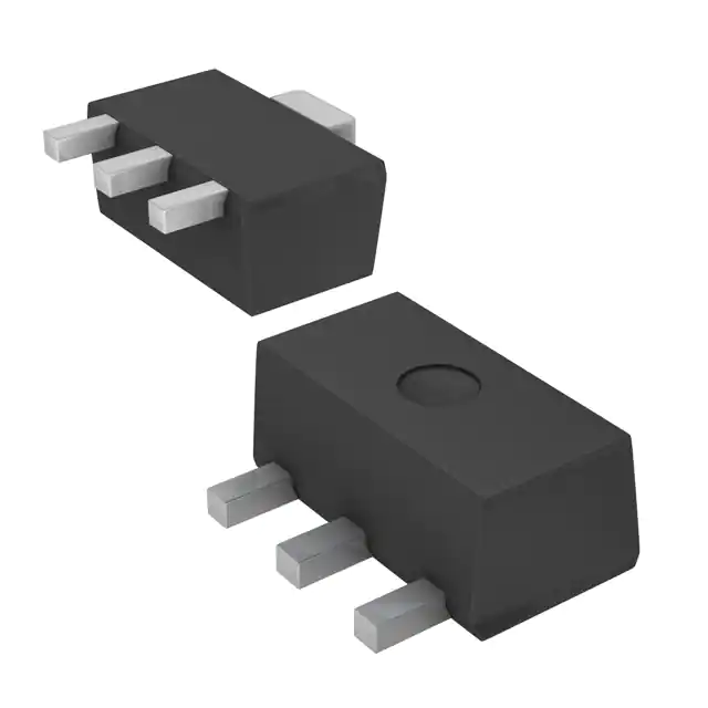
SOT89-3L
Mechanical Data
•
•
•
•
•
•
•
Case: SOT89-3L
Case Material: Molded Plastic, "Green” Molding Compound.
UL Flammability Classification Rating 94V-0
Moisture Sensitivity: Level 1 per J-STD-020C
Terminals: Finish — Matte Tin annealed over Copper leadframe
(Lead Free Plating). Solderable per MIL-STD-202, Method 208
Marking & Type Code Information: See Page 3
Ordering Information: See Page 3
Weight: 0.072 grams (approximate)
Maximum Ratings
3 E
2 C
C 4
1 B
COLLECTOR
2,4
1
BASE
3
EMITTER
Schematic and Pin Configuration
TOP VIEW
@TA = 25°C unless otherwise specified
Characteristic
Symbol
VCBO
VCEO
VEBO
IC
ICM
Collector-Base Voltage
Collector-Emitter Voltage
Emitter-Base Voltage
Collector Current
Peak Pulse Current
Value
100
80
5
1
1.5
Unit
V
V
V
A
A
Symbol
PD
Value
1
Unit
W
Tj, TSTG
-55 to +150
°C
RθJA
125
°C/W
Thermal Characteristics
Characteristic
Power Dissipation (Note 3) @ TA = 25°C
Operating and Storage Temperature Range
Thermal Resistance, Junction to Ambient Air (Note 3) @TA = 25°C
Electrical Characteristics
@TA = 25°C unless otherwise specified
Characteristic
OFF CHARACTERISTICS (Note 4)
Collector-Base Breakdown Voltage
Collector-Emitter Breakdown Voltage
Emitter-Base Breakdown Voltage
Symbol
Min
Typ
Max
Unit
V(BR)CBO
V(BR)CEO
V(BR)EBO
100
80
5.0
⎯
⎯
⎯
V
V
V
Collector-Base Cutoff Current
ICBO
⎯
⎯
Emitter-Base Cutoff Current
ON CHARACTERISTICS (Note 4)
IEBO
⎯
⎯
⎯
⎯
⎯
0.1
20
100
⎯
VCE(SAT)
VBE(ON)
63
40
63
100
⎯
⎯
fT
Cobo
DCX56, DCX56-16
DC Current Gain
Collector-Emitter Saturation Voltage
Base-Emitter Turn-On Voltage
SMALL SIGNAL CHARACTERISTICS
Current Gain-Bandwidth Product
Output Capacitance
Notes:
1.
2.
3.
4.
DCX56
DCX56-16
hFE
μA
nA
⎯
⎯
⎯
⎯
⎯
⎯
250
250
0.5
1.0
⎯
⎯
V
V
⎯
200
⎯
MHz
⎯
⎯
15
pF
⎯
Test Conditions
IC = 100μA, IE = 0
IC = 10mA, IB = 0
IE = 10μA, IC = 0
VCB = 30V, IE = 0
VCB = 30V, IE = 0, TA = 150°C
VEB = 5.0V, IC = 0
IC = 5.0mA, VCE = 2.0V
IC = 500mA, VCE = 2.0V
IC = 150mA, VCE = 2.0V
IC = 150mA, VCE = 2.0V
IC = 500mA, IB = 50mA
IC = 500mA, VCE = 2.0V
IC = 50mA, VCE = 5V,
f = 100MHz
VCB = 10V, IE = 0, f = 1MHz
No purposefully added lead.
Diodes Inc.'s "Green" policy can be found on our website at http://www.diodes.com/products/lead_free/index.php.
Device mounted on FR-4 PCB; pad layout as shown on page 4 or in Diodes Inc. suggested pad layout document AP02001, which can
be found on our website at http://www.diodes.com/datasheets/ap02001.pdf.
Measured under pulsed conditions. Pulse width = 300μs. Duty cycle ≤2%.
DS31161 Rev. 3 - 2
1 of 4
www.diodes.com
DCX56/-16
© Diodes Incorporated
�IC, COLLECTOR CURRENT (A)
NEW PRODUCT
VCE(SAT), COLLECTOR EMITTER
SATURATION VOLTAGE (V)
VCE, COLLECTOR EMITTER VOLTAGE (V)
IC, COLLECTOR CURRENT (A)
DS31161 Rev. 3 - 2
VBE(SAT), BASE EMITTER SATURATION VOLTAGE (V)
VBE(ON), BASE EMITTER TURN-ON VOLTAGE (V)
IC, COLLECTOR CURRENT (A)
2 of 4
www.diodes.com
IC, COLLECTOR CURRENT (A)
DCX56/-16
© Diodes Incorporated
�CAPACITANCE (pF)
NEW PRODUCT
VCE = 5V
f = 100MHz
VR, REVERSE VOLTAGE (V)
Fig. 8 Typical Gain-Bandwidth Product
vs. Collector Current
Ordering Information (Note 5)
Device
DCX56-13
DCX56-16-13
Notes:
5.
Packaging
SOT89-3L
SOT89-3L
Shipping
2500/Tape & Reel
2500/Tape & Reel
For packaging details, go to our website at http://www.diodes.com/ap02007.pdf.
Marking Information
(Top View)
XXX = Product Type Marking Code ex. N18 = DCX56
N18-16 = DCX56-16
= Manufacturer’s code marking
YWW = Date Code Marking
Y = Last digit of year ex: 7 = 2007
WW = Week code 01 - 52
YWW
XXX
Package Outline Dimensions
SOT89-3L
0
20
0.
R
D1
C
Dim
E
H
L
B
B1
8°
Max
Typ
A
1.40
1.60
1.50
B
0.45
0.55
0.50
B1
0.37
0.47
0.42
C
0.35
0.43
0.38
D
4.40
4.60
4.50
D1
1.50
1.70
1.60
E
2.40
2.60
2.50
e
—
—
1.50
e
(4X
)
A
H
3.95
4.25
4.10
L
0.90
1.20
1.05
All Dimensions in mm
D
DS31161 Rev. 3 - 2
Min
3 of 4
www.diodes.com
DCX56/-16
© Diodes Incorporated
�Suggested Pad Layout
NEW PRODUCT
1.7
2.7
0.4
1.9
1.3
0.9
3.0
Unit: mm
IMPORTANT NOTICE
Diodes Incorporated and its subsidiaries reserve the right to make modifications, enhancements, improvements, corrections or other changes
without further notice to any product herein. Diodes Incorporated does not assume any liability arising out of the application or use of any product
described herein; neither does it convey any license under its patent rights, nor the rights of others. The user of products in such applications shall
assume all risks of such use and will agree to hold Diodes Incorporated and all the companies whose products are represented on our website,
harmless against all damages.
LIFE SUPPORT
Diodes Incorporated products are not authorized for use as critical components in life support devices or systems without the expressed written
approval of the President of Diodes Incorporated.
DS31161 Rev. 3 - 2
4 of 4
www.diodes.com
DCX56/-16
© Diodes Incorporated
�
很抱歉,暂时无法提供与“DCX56-16-13”相匹配的价格&库存,您可以联系我们找货
免费人工找货