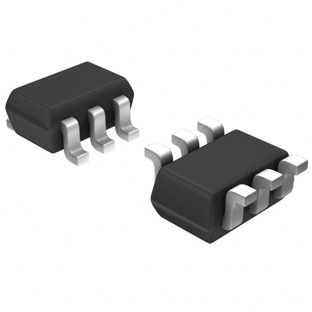
DDC144TU
DUAL NPN TRANSISTORS WITH 47K OHM BASE RESISTOR
Please click here to visit our online spice models database.
General Description
NEW PRODUCT
•
DDC144TU is best suited for logic switching applications
using control circuits like micro-controllers, comparators,
etc. It features two discrete NPN transistors which can
support maximum continuous current of 100 mA. NPN
transistors can be used as a control and also these can
be biased using higher supply voltages due to the built in
current limiting base resistor of 47 K Ohm. The
component devices can be used as a part of a circuit or
as a stand alone discrete device.
Fig. 1: SOT-363
Features
•
•
•
•
Built in Base Resistors
Epitaxial Planar Die Construction
Lead Free By Design/RoHS Compliant (Note 1)
"Green" Device (Note 2)
BQ2
CQ1
Mechanical Data
•
•
•
•
•
•
•
•
EQ2
47k
R2
DDC144T_DIE
Case: SOT-363
Case Material: Molded Plastic. "Green Molding"
Compound. UL Flammability Classification Rating 94V-0
Moisture Sensitivity: Level 1 per J-STD-020C
Terminal Connections: See Fig. 2
Terminals: Finish - Matte Tin annealed over Alloy 42
leadframe. Solderable per MIL-STD-202, Method 208
Marking & Type Code Information: See Page 5
Ordering Information: See Page 5
Weight: 0.015 grams (approximate)
Q2
DDC144T_DIE
Q1
R1 47k
BQ1
EQ1
CQ2
Fig. 2: Schematic and Pin Configuration
Sub-Component P/N
Reference
Device Type
R1 (NOM)
R2 (NOM)
Figure
DDTC144T_DIE
Q1
NPN
47KΩ
⎯
2
DDTC144T_DIE
Q2
NPN
⎯
47KΩ
2
Maximum Ratings: Total Device
@TA = 25°C unless otherwise specified
Characteristic
Power Dissipation
Symbol
Value
Unit
Pd
200
mW
Power Deration above 25°C
Pder
1.6
mW / °C
Output Current
Iout
100
mA
Thermal Characteristics
Characteristic
Junction Operation and Storage Temperature Range
Thermal Resistance, junction to ambient (packaged device)
(Ref: equivalent to only one heated junction) @ TA = 25°C
Notes:
Symbol
Value
Unit
TJ, TSTG
-55 to +150
°C
RθJA
625
°C/W
1. No purposefully added lead.
2. Diodes Inc.'s "Green" policy can be found on our website at http:/www.diodes.com/products/lead_free/index.php.
3. Device mounted on FR-4 PCB, 1" x 0.85" x 0.062"; pad layout as shown on Page 5 or see Diodes Inc. suggested pad layout document AP02001, which
can be found on our website at http:/www.diodes.com/datasheets/ap02001.pdf.
DS30767 Rev. 7 - 2
1 of 6
www.diodes.com
DDC144TU
© Diodes Incorporated
�Maximum Ratings:
Sub-Component Device: Discrete NPN Transistor (Q1, Q2)
NEW PRODUCT
Characteristic
Collector-Base Voltage
@TA = 25°C unless otherwise specified
Symbol
VCBO
Value
50
Collector-Emitter Voltage
VCEO
50
V
Emitter-Base Voltage
VEBO
6
V
Collector Current (dc)
IC(max)
50
mA
Electrical Characteristics
Unit
V
@TA = 25°C unless otherwise specified
Characteristic
Off Characteristics
Collector-Base Cut Off Current
Collector-Emitter Cut Off Current, IO(OFF)
Emitter-Base Cut Off Current
Symbol
Min
Typ
Max
Unit
ICBO
⎯
⎯
100
nA
VCB = 50V, IE = 0
ICEO
⎯
⎯
500
nA
VCE = 50V, IB = 0
IEBO
⎯
500
nA
VEB = 5V, IC = 0
⎯
⎯
V
IC = 50uA, IE = 0
IC = 1 mA, IB = 0
Collector-Base Breakdown Voltage
V(BR)CBO
⎯
50
Collector-Emitter Breakdown Voltage
Test Condition
V(BR)CEO
50
⎯
⎯
V
Emitter-Base Breakdown Voltage
V(BR)EBO
6
⎯
V
IE = 50uA, IC = 0
Output Voltage (Transistor is off)
VOH
4.6
⎯
4.45
V
VCC = 5V, VB = 0.05V, RL = 1KΩ
VI(OFF)
⎯
0.6
⎯
0.4
⎯
850
⎯
nA
VCE = 5V, IC = 100uA
IO(OFF)
⎯
⎯
0.03
0.1
V
IC = 2.5 mA, IB = 0.25 mA
⎯
0.075
0.1
V
IC = 10mA, IB = 0.5mA
⎯
0.05
0.1
V
IC = 10mA, IB = 1mA
⎯
150
0.2
0.3
V
IC = 50mA, IB= 5mA
400
⎯
⎯
VCE = 5V, IC = 1 mA
150
400
⎯
⎯
VCE = 5V, IC = 10 mA
150
350
⎯
⎯
VCE = 5V, IC = 25 mA
150
300
⎯
⎯
VCE = 5V, IC = 50 mA
50
110
⎯
Vdc
VCE = 5V, IC = 100 mA
VCC = 5V, VB = 2.5V, RL=10KΩ
VI(ON)
⎯
1.5
⎯
0.25
0.95
Vdc
VO= 0.3V, IC= 2mA
Ii
⎯
19.2
⎯
28
mA
VI = 5V
Base-Emitter Turn-on Voltage
VBE(ON)
⎯
⎯
1.2
V
VCE = 5V, IC = 2mA
Base-Emitter Saturation Voltage
Input Resistor +/- 30% (Base)
Small Signal Characteristics
Transition Frequency (gain-bandwidth product)
VBE(SAT)
R1
⎯
⎯
⎯
47
1.6
⎯
V
KΩ
IC = 200uA, IB = 20uA
⎯
fT
⎯
250
VCE = 10V, IE = 5mA, f =100MHz
⎯
⎯
⎯
5
MHz
CC
pF
VCB = 10V, IE = 0, f = 1MHz
Input Voltage (load is off)
Output Current (leakage same as ICEO)
On Characteristics*
Collector-Emitter Saturation Voltage
DC Current Gain
Output Voltage (equivalent to VCE(SAT) or VO(on))
Input Voltage
Input Current
Collector Capacitance, (Ccbo-Output Capacitance)
VCE(SAT)
hFE
VOL
0.2
VCC = 50V, VI = 0V
*Pulse Test: Pulse width, tp
很抱歉,暂时无法提供与“DDC144TU-7”相匹配的价格&库存,您可以联系我们找货
免费人工找货- 国内价格
- 20+0.46215
- 40+0.44701
- 80+0.43942
- 160+0.41669
- 国内价格
- 1+0.59840
- 200+0.38610
- 1500+0.33550
- 3000+0.29700