NOT RECOMMENDED FOR NEW DESIGN
USE DMP1007UCB9
DMP1012UCB9
P-CHANNEL ENHANCEMENT MODE MOSFET
Product Summary (Typ. @ VGS = -4.5V, TA
Features
= +25°C)
NEW PRODUCT
INFORMATION
ADVANCED
ADVANCE INFORMATION
VDSS
RDS(ON)
Qg
Qgd
ID
-8V
8.2mΩ
8.1nC
1.8nC
-10A
Description
This 3rd generation Lateral MOSFET (LD-MOS) is engineered to
minimize on-state losses and switch ultra-fast, making it ideal for high
efficiency power transfer. It uses Chip-Scale Package (CSP) to
increase power density by combining low thermal impedance with
minimal RDS(ON) per footprint area.
LD-MOS Technology with the Lowest Figure of Merit:
RDS(ON) = 8.2mΩ to Minimize On-State Losses
Qg = 8.1nC for Ultra-Fast Switching
Vgs(th) = -0.8V Typ. for a Low Turn-On Potential
CSP with Footprint 1.5mm × 1.5mm
Height = 0.62mm for Low Profile
ESD = 6kV HBM Protection of Gate
Totally Lead-Free & Fully RoHS Compliant (Notes 1 & 2)
Halogen and Antimony Free. “Green” Device (Note 3)
Qualified to AEC-Q101 Standards for High Reliability
Applications
Mechanical Data
DC-DC Converters
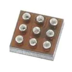
Case: U-WLB1515-9
Battery Management
Terminal Connections: See Diagram Below
Load Switch
U-WLB1515-9
G
S
S
S
S
S
D
D
D
Top-View
Pin Configuration
Equivalent Circuit
Ordering Information (Note 4)
Part Number
DMP1012UCB9-7
Notes:
Case
U-WLB1515-9
Packaging
3,000/Tape & Reel
1. No purposely added lead. Fully EU Directive 2002/95/EC (RoHS), 2011/65/EU (RoHS 2) & 2015/863/EU (RoHS 3) compliant.
2. See https://www.diodes.com/quality/lead-free/ for more information about Diodes Incorporated’s definitions of Halogen- and Antimony-free, "Green" and
Lead-free.
3. Halogen- and Antimony-free "Green” products are defined as those which contain
很抱歉,暂时无法提供与“DMP1012UCB9-7”相匹配的价格&库存,您可以联系我们找货
免费人工找货- 国内价格 香港价格
- 3000+2.603243000+0.33662
- 6000+2.408096000+0.31139
- 9000+2.308699000+0.29854
- 15000+2.2865915000+0.29568