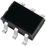
LMN200B02-7

LMN200B02-7

  • 厂商:

    BCDSEMI(美台)

  • 封装:

    TSSOP6,SC88,SOT363

  • 描述:

    PNP三极管+N沟道MOSFET

  • 详情介绍
  • 数据手册
  • 价格&库存
LMN200B02-7 数据手册
LMN200B02 PART OBSOLETE - CONTACT US 200 mA LOAD SWITCH FEATURING PRE-BIASED PNP TRANSISTOR AND N-MOSFET WITH GATE PULL DOWN RESISTOR OBSOLETE – PART DISCONTINUED General Description LMN200B02 is best suited for applications where the load needs to be turned on and off using control circuits like micro-controllers, comparators etc. particularly at a point of load. It features a discrete pass transistor with stable VCE(SAT) which does not depend on the input voltage and can support continuous maximum current of 200 mA . It also contains a discrete N-MOSFET that can be used as control. This N-MOSFET also has a built-in pull down resistor at its gate. The component can be used as a part of a circuit or as a stand alone discrete device. 6 5 4 1 2 3 Features • • • • • • Fig. 1: SOT-363 Voltage Controlled Small Signal Switch N-MOSFET with Gate Pull-Down Resistor Surface Mount Package Ideally Suited for Automated Assembly Processes Lead Free By Design/RoHS Compliant (Note 1) "Green" Device (Note 2) • • • • • • B_Q1 S_Q2 6 5 4 Q1 Mechanical Data • • C_Q1 PNP C DDTB142JU_DIE R2 B R3 470 37K E Case: SOT-363 Case Material: Molded Plastic, “Green” Molding Compound. UL Flammability Classification Rating 94V-0 Moisture Sensitivity: Level 1 per J-STD-020 Terminal Connections: See Diagram Terminals: Finish - Matte Tin annealed over Alloy 42 leadframe. Solderable per MIL-STD-202, Method 208 Marking Information: See Page 8 Ordering Information: See Page 8 Weight: 0.006 grams (approximate) R1 S G 10K Q2 NMOS DSNM6047_DIE D 1 2 3 E_Q1 G_Q2 D_Q2 Fig. 2 Schematic and Pin Configuration Sub-Component P/N Reference Device Type R1 (NOM) R2 (NOM) R3 (NOM) Figure DDTB142JU_DIE DSNM6047_DIE (with Gate Pull-Down Resistor) Q1 PNP Transistor 10K 470  2 Q2 N-MOSFET   37K 2 Maximum Ratings, Total Device @TA = 25°C unless otherwise specified Symbol Value Power Dissipation (Note 3) Characteristic PD 200 mW Power Derating Factor above 125°C Pder 1.6 mW/°C Output Current Iout 200 mA Symbol Value Unit TJ,TSTG -55 to +150 °C RθJA 625 °C/W Thermal Characteristics @TA = 25°C unless otherwise specified Characteristic Operating and Storage Temperature Range Thermal Resistance, Junction to Ambient Air (Equivalent to One Heated Junction of PNP Transistor) (Note 3) Notes: Unit 1. No purposefully added lead. 2. Diodes Inc.'s "Green" policy can be found on our website at http://www.diodes.com/products/lead_free/index.php. 3. Device mounted on FR-4 PCB, 1 inch x 0.85 inch x 0.062 inch; pad layout as shown on Diodes Inc. suggested pad layout document AP02001, which can be found on our website at http://www.diodes.com/datasheets/ap02001.pdf. LMN200B02 Document number: DS30658 Rev. 8 - 4 1 of 11 www.diodes.com October 2021 © Diodes Incorporated Maximum Ratings: Sub-Component Device: Pre-Biased PNP Transistor (Q1) OBSOLETE – PART DISCONTINUED Characteristic @TA = 25°C unless otherwise specified Symbol Value Unit Collector-Base Voltage VCBO -50 V Collector-Emitter Voltage VCEO -50 V Supply Voltage VCC -50 V Input Voltage Vin +5 to -6 V Output Current IC -200 mA Sub-Component Device: N-MOSFET With Gate Pull-Down Resistor (Q2) @TA = 25°C unless otherwise specified Symbol Value Unit Drain-Source Voltage Characteristic VDSS 60 V Drain Gate Voltage (RGS ≤1M Ohm) VDGR 60 V Gate-Source Voltage Drain Current (Page 1: Note 3) Continuous Pulsed (tp
LMN200B02-7
根据您提供的PDF文档,以下是中文翻译和分析的结果:

物料型号:ATMEGA328P-AU 器件简介:ATMEGA328P-AU是一款低功耗、高性能的8位AVR微控制器,适用于各种嵌入式系统。

引脚分配:该芯片有44个引脚,包括电源引脚、地引脚、复位引脚、I/O引脚等。

参数特性:工作电压为1.8-5.5V,工作频率为16MHz,具有32KB的闪存和2KB的SRAM。

功能详解:ATMEGA328P-AU具有多种功能,包括通用I/O引脚、定时器/计数器、中断、模拟-数字转换器等。

应用信息:广泛应用于工业控制、消费电子、医疗设备等领域。

封装信息:采用TQFP封装,共有44个引脚。

LMN200B02-7 价格&库存

很抱歉,暂时无法提供与“LMN200B02-7”相匹配的价格&库存,您可以联系我们找货

免费人工找货