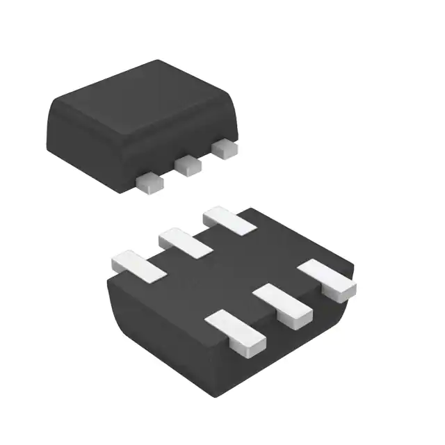
MMDT3906VC
NEW PRODUCT
Lead-free Green
DUAL PNP SMALL SIGNAL SURFACE MOUNT
TRANSISTOR
Features
•
•
•
•
•
Epitaxial Planar Die Construction
A
Ideal for Low Power Amplification and Switching
B2
C1
Ultra-Small Surface Mount Package
E2
SOT-563
Lead Free By Design/RoHS Compliant (Note 1)
B C
"Green" Device (Note 4)
E1
Mechanical Data
•
•
•
•
•
•
•
•
C2
B1
D
G
Case: SOT-563
Case Material: Molded Plastic, "Green" Molding Compound.
UL Flammability Classification Rating 94V-0
Min
Max
Typ
A
0.15
0.30
0.25
B
1.10
1.25
1.20
C
1.55
1.70
1.60
D
M
K
Moisture Sensitivity: Level 1 per J-STD-020C
Terminal Connections: See Diagram
H
Terminals: Finish - Matte Tin annealed over Copper
leadframe. Solderable per MIL-STD-202, Method 208
L
SEE NOTE 2
Marking & Type Code Information: See Last Page
Ordering Information: See Last Page
Dim
0.50
G
0.90
1.10
1.00
H
1.50
1.70
1.60
K
0.56
0.60
0.60
L
0.10
0.30
0.20
M
0.10
0.18
All Dimensions in mm
C1
B2
E2
E1
B1
C2
Weight: 0.003 grams (approximate)
Maximum Ratings
@ TA = 25°C unless otherwise specified
Symbol
Value
Unit
Collector-Base Voltage
Characteristic
VCBO
-40
V
Collector-Emitter Voltage
VCEO
-40
V
Emitter-Base Voltage
VEBO
-5.0
V
IC
-200
mA
Collector Current - Continuous
Power Dissipation (Note 3)
Thermal Resistance, Junction to Ambient
Operating and Storage and Temperature Range
Thermal Characteristics
150
mW
833
°C/W
Tj, TSTG
-55 to +150
°C
Symbol
Value
Unit
Pd
150
mW
RθJA
833
°C/W
@ TA = 25°C unless otherwise specified
Characteristic
Power Dissipation (Note 3)
Thermal Resistance, Junction to Ambient
Notes:
Pd
RθJA
1. No purposefully added lead.
2. Package is non-polarized. Parts may be on reel in orientation illustrated, 180° rotated, or mixed (both ways).
3. Device mounted on FR-4 PCB, 1 inch x 0.85 inch x 0.062 inch; pad layout as shown on Diodes Inc. suggested pad layout
document AP02001, which can be found on our website at http://www.diodes.com/datasheets/ap02001.pdf.
4. Diodes Inc's "Green" policy can be found on our website at http://www.diodes.com/products/lead_free/index.php
DS30640 Rev. 3 - 2
1 of 4
www.diodes.com
MMDT3906VC
Diodes Incorporated
�NEW PRODUCT
Electrical Characteristics
@ TA = 25°C unless otherwise specified
Characteristic
Symbol
Min
Max
Unit
Test Condition
Collector-Base Breakdown Voltage
V(BR)CBO
-40
V
IC = -10µA, IE = 0
Collector-Emitter Breakdown Voltage
V(BR)CEO
-40
V
IC = -1.0mA, IB = 0
Emitter-Base Breakdown Voltage
V(BR)EBO
-5.0
V
IE = -10µA, IC = 0
ICEX
-50
nA
VCE = -30V, VEB(OFF) = -3.0V
IBL
-50
nA
VCE = -30V, VEB(OFF) = -3.0V
hFE
60
80
100
60
30
300
IC = -100µA, VCE =
IC = -1.0mA, VCE =
IC = -10mA, VCE =
IC = -50mA, VCE =
IC = -100mA, VCE =
Collector-Emitter Saturation Voltage
VCE(SAT)
-0.25
-0.40
V
IC = -10mA, IB = -1.0mA
IC = -50mA, IB = -5.0mA
Base-Emitter Saturation Voltage
VBE(SAT)
-0.65
-0.85
-0.95
V
IC = -10mA, IB = -1.0mA
IC = -50mA, IB = -5.0mA
Output Capacitance
Cobo
4.5
pF
VCB = -5.0V, f = 1.0MHz, IE = 0
Input Capacitance
Cibo
10
pF
VEB = -0.5V, f = 1.0MHz, IC = 0
Input Impedance
hie
2.0
12
kΩ
Voltage Feedback Ratio
hre
0.1
10
x 10-4
Small Signal Current Gain
hfe
100
400
Output Admittance
hoe
3.0
60
µS
Current Gain-Bandwidth Product
fT
250
MHz
VCE = -20V, IC = -10mA,
f = 100MHz
Noise Figure
NF
4.0
dB
VCE = -5.0V, IC = -100µA,
RS = 1.0kΩ, f = 1.0kHz
Delay Time
td
35
ns
Rise Time
tr
35
ns
Storage Time
ts
225
ns
Fall Time
tf
75
ns
OFF CHARACTERISTICS (Note 5)
Collector Cutoff Current
Base Cutoff Current
ON CHARACTERISTICS (Note 5)
DC Current Gain
-1.0V
-1.0V
-1.0V
-1.0V
-1.0V
SMALL SIGNAL CHARACTERISTICS
VCE = 10V, IC = 1.0mA,
f = 1.0kHz
SWITCHING CHARACTERISTICS
Notes:
VCC = -3.0V, IC = -10mA,
VBE(off) = 0.5V, IB1 = -1.0mA
VCC = -3.0V, IC = -10mA,
IB1 = IB2 = -1.0mA
5. Short duration test pulse used to minimize self-heating.
DS30640 Rev. 3 - 2
2 of 4
www.diodes.com
MMDT3906VC
�100
CIBO, INPUT CAPACITANCE (pF)
COBO, OUTPUT CAPACITANCE (pF)
Pd, POWER DISSIPATION (mW)
f = 1MHz
200
150
100
50
10
Cibo
Cobo
1
0.1
0
-50
0
50
100
150
1000
10
100
10
VCE(SAT), COLLECTOR-EMITTER (V)
SATURATION VOLTAGE
hFE, DC CURRENT GAIN
1
VCB, COLLECTOR-BASE VOLTAGE (V)
Fig. 2, Input and Output Capacitance vs.
Collector-Base Voltage
TA, AMBIENT TEMPERATURE (°C)
Fig. 1, Derating Curve - Total
TA = 125°C
100
TA = +25°C
TA = -25°C
10
IC
IB = 10
1
0.1
VCE = 1.0V
1
0.01
1
0.1
10
100
1000
1
IC, COLLECTOR CURRENT (mA)
Fig. 3, Typical DC Current Gain vs
Collector Current
10
100
1000
IC, COLLECTOR CURRENT (mA)
Fig. 4, Typical Collector-Emitter Saturation Voltage
vs. Collector Current
1.0
VBE(SAT), BASE-EMITTER (V)
SATURATION VOLTAGE
NEW PRODUCT
250
0.9
0.8
0.7
0.6
IC
IB = 10
0.5
1
10
100
IC, COLLECTOR CURRENT (mA)
Fig. 5, Typical Base-Emitter
Saturation Voltage vs. Collector Current
DS30640 Rev. 3 - 2
3 of 4
www.diodes.com
MMDT3906VC
�NEW PRODUCT
Ordering Information
Notes:
(Note 6)
Device
Packaging
Shipping
MMDT3906VC-7
SOT-563
3000/Tape & Reel
6. For Packaging Details, go to our website at http://www.diodes.com/datasheets/ap02007.pdf.
Marking Information
ARK = Product Type Marking Code
YM = Date Code Marking
Y = Year ex: R = 2004
M = Month ex: 9 = September
ARK YM
Date Code Key
Year
2004
2005
2006
2007
2008
2009
Code
R
S
T
U
V
W
Month
Jan
Feb
March
Apr
May
Jun
Jul
Aug
Sep
Oct
Nov
Dec
Code
1
2
3
4
5
6
7
8
9
O
N
D
DS30640 Rev. 3 - 2
4 of 4
www.diodes.com
MMDT3906VC
�