NOT RECOMMENDED FOR NEW DESIGN
USE ZXLD1371
PAM2842
HIGH POWER LED DRIVER
Description
Pin Assignments
The PAM2842 is a high power LED driver, capable of driving up to 10
high power LEDs in series. The PAM2842 supports buck, boost and
sepic topology.
The PAM2842 features over current protection, over voltage
protection, under voltage lockout and over temperature protection,
which prevent the device from damage.
LED dimming can be done by using a PWM signal to the COMP pin.
The PAM2842 is available in TSSOP-20 packages.
Features
Output Power up to 30W
Chip Enable with Soft-start
Analog and PWM Dimming
Peak Efficiency up to 97%
Low Quiescent Current
Switching Frequency Adjustable
Support Buck/Boost/Sepic Toplogy
Over Current Protection
Over Voltage Protection
Thermal Protection
UVLO
Tiny Pb-Free Packages: 40-Pin QFN6x6 and TSSOP-20
Applications
PAM2842
Document number: DS36412 Rev. 2 - 3
Home Lighting
Automotive Lighting
Monitor Backlighting
1 of 17
www.diodes.com
April 2018
© Diodes Incorporated
�NOT RECOMMENDED FOR NEW DESIGN
USE ZXLD1371
PAM2842
Typical Applications Circuit
Boost with Low Side Current Sense
Boost with High Side Current Sense
Buck/Boost (Sepic) with Low Side Current Sense
Buck/Boost (Sepic) with High Side Current Sense
Buck with High Side Current Sense
PAM2842
Document number: DS36412 Rev. 2 - 3
2 of 17
www.diodes.com
April 2018
© Diodes Incorporated
�NOT RECOMMENDED FOR NEW DESIGN
USE ZXLD1371
PAM2842
Pin Descriptions
Pin
Name
PGND
HVIN
EN
VDD-DR
RT
AGND
SenseSense+
COMP
VDD_5V
OV
SW
NC
Pin Number
QFN6x6-40
TSSOP-20
1–6
1, 2, 3, 4, 10, 11
8
5
9
6
10
7
12
8
13
9
14
12
15
13
17
14
21
15
23
16
25 – 30
17, 18, 19
7, 11, 16, 18-20,
20
22, 24, 31-40
Function
Power Ground
Input
Chip Enable, Active High
Internal LDO Output
Frequency Adjustment Pin
Analog Ground
Sense Resistor Sense Resistor+
Compensation Node
Internal LDO Output
Over Voltage
Drain of Main Switch
Not Connected
Functional Block Diagram
PAM2842
Document number: DS36412 Rev. 2 - 3
3 of 17
www.diodes.com
April 2018
© Diodes Incorporated
�NOT RECOMMENDED FOR NEW DESIGN
USE ZXLD1371
PAM2842
Absolute Maximum Ratings (@TA = +25°C, unless otherwise specified.)
These are stress ratings only and functional operation is not implied. Exposure to absolute maximum ratings for prolonged time periods may
affect device reliability. All voltages are with respect to ground.
Parameter
Supply Voltage
Buck Application Maximum Output Current
I/O Pin Voltage Range
Rating
40
3
Unit
V
A
GND -0.3 to VDD +0.3
V
150
-40 to +150
300, 5s
°C
Maximum Junction Temperature
Storage Temperature
Soldering Temperature
Recommended Operating Conditions (@TA = +25°C, unless otherwise specified.)
Parameter
Supply Voltage Range
Operation Temperature Range
Junction Temperature Range
Rating
Unit
5.5 to 40
-40 to +85
-40 to +125
V
°C
Thermal Information
Parameter
Thermal Resistance
(Junction to Case)
Thermal Resistance
(Junction to Ambient)
Note:
Package
TSSOP-20
QFN6x6-40
TSSOP-20
QFN6x6-40
Symbol
θJC
θJA
Max
Unit
20
7.6 (Note 1)
°C/W
90
18.1 (Note 1)
1. The exposed PAD must be soldered to a thermal land on the PCB.
Electrical Characteristics (@TA = +25°C, VEN = VDD = 24V, 1W x 10 LEDs, unless otherwise specified.)
Parameter
Input Voltage Range
Quiescent Current
E NA = high (no switching frequency)
E NA = high (1M switching frequency)
E NA = high (500k switching frequency)
E NA = high (200k switching frequency)
E NA = low
Min
5.5
-
Typ
1
6
3
1.6
5
Max
40
2
10
Unit
V
mA
mA
mA
mA
µA
Feedback Voltage, Low Side
VFB = VSENSE+ -AGND, VSENSE- = AGND
95
100
105
mV
Feedback Voltage, High Side
VFB = VSENSE+ – VSENSE-
95
100
105
mV
LED Current Line Regulation
IO = 350mA
-
0.02
-
%/V
LED Current Load Regulation
VDD_DR UVLO Hysteresis
No Switching
-
1.0
200
-
%
mV
PAM2842
Document number: DS36412 Rev. 2 - 3
Test Conditions
4 of 17
www.diodes.com
April 2018
© Diodes Incorporated
�NOT RECOMMENDED FOR NEW DESIGN
USE ZXLD1371
PAM2842
Electrical Characteristics (cont.) (@TA = +25°C, VEN = VDD = 24V, 1W x 10 LEDs, unless otherwise specified.)
Parameter
Test Conditions
Min
Typ
Max
Units
LDO Stage
VDD_5V
VDD_5V Current Limit
VDD_5V UVLO Threshold
VDD_5V UVLO Hysteresis
VDD_DR
VDD_DR Current_Limit
VDD_DR UVLO Threshold
Switch Stage
Switch RDS(ON)
Switch Current Limit
Switch Leakage Current
No Switching
No Switching
No Switching
No Switching
No Switching
No Switching
No Switching
4.5
14
3.7
4.5
14
3.7
5
74
4.0
200
5
50
4.0
5.5
90
4.3
5.5
90
4.3
V
mA
V
mV
V
mA
V
VDD_5V = 5V
-
-
0.1
3.5
50
-
Ω
A
µA
RT Voltage
RRT = 71kΩ
1.1
1.2
1.3
V
RRT = 30kΩ
800k
1M
1.2M
Hz
RRT = 71kΩ
400
500
600
kHz
RRT = 180kΩ
160
200
240
kHz
FSW = 1MHz
-
10
-
%
FSW = 500kHz
-
5
-
%
FSW = 200kHz
-
2.5
-
%
Low Side Sense
High Side Sense
Feedback Voltage = 0
Feedback Voltage = 0
-
95
100
30
30
-
%
%
µA
µA
Switching Frequency (Note 2)
Min Duty Cycle
Max Duty Cycle
VC Source Current
VC Sink Current
Fault Protection
OV Threshold Voltage
OV Hysteresis
Thermal Shutdown
Thermal Shutdown Hysteresis
Control Interface
-
1.1
-
1.2
70
+150
+30
1.3
-
V
mV
°C
°C
EN High
EN Low
-
1.5
-
-
0.4
V
V
Note:
2. Switching frequency
FSW
PAM2842
Document number: DS36412 Rev. 2 - 3
1012
24 x(RRT 12k )
, reference value.
5 of 17
www.diodes.com
April 2018
© Diodes Incorporated
�NOT RECOMMENDED FOR NEW DESIGN
USE ZXLD1371
PAM2842
Typical Performance Characteristics
Boost Mode, @TA = +25°C, VEN = VDD = 24V, 3W LEDs, FSW = 200kHz, unless otherwise specified.)
PAM2842
Document number: DS36412 Rev. 2 - 3
6 of 17
www.diodes.com
April 2018
© Diodes Incorporated
�NOT RECOMMENDED FOR NEW DESIGN
USE ZXLD1371
PAM2842
Typical Performance Characteristics (cont.) @TA = +25°C, FSW = 300kHz, unless otherwise specified.)
PAM2842
Document number: DS36412 Rev. 2 - 3
7 of 17
www.diodes.com
April 2018
© Diodes Incorporated
�NOT RECOMMENDED FOR NEW DESIGN
USE ZXLD1371
PAM2842
Application Information
Topology Selection
When maximum power supply voltage is below than minimum load voltage, select the boost topology. When minimum power supply voltage is
high than maximum load voltage, select buck topology. When load voltage range is small and between the power supply voltage, select sepic
topology.
Table 1: Voltage Condition vs. Topology
Condition
Topology
VINMAX < VOMIN
Boost
VINMIN > VOMAX
Buck
VO
很抱歉,暂时无法提供与“PAM2842TJR”相匹配的价格&库存,您可以联系我们找货
免费人工找货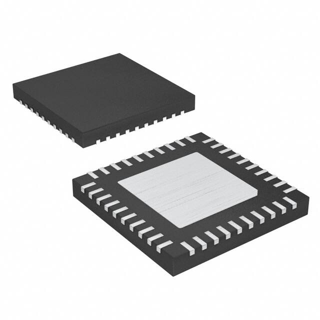


 工商网监
湘ICP备2023018690号
工商网监
湘ICP备2023018690号
