NOT RECOMMENDED FOR NEW DESIGN
USE AP2127N/K/AP2125KS
PAM3103
300mA ADJUSTABLE HIGH PSRR CMOS LINEAR REGULATOR
Description
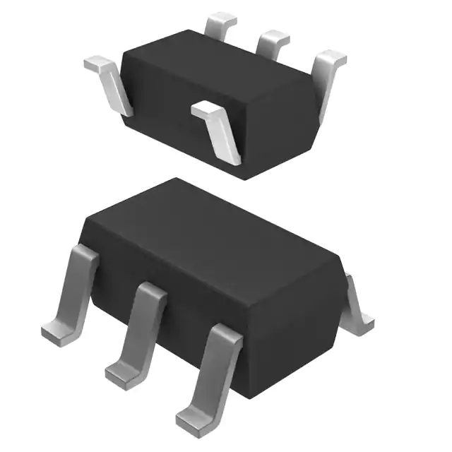
Pin Assignments
The PAM3103 is a positive, adjustable linear regulator. It features low
quiescent current (65µA typ.) and low dropout voltage, making it ideal
for battery powered applications. The output voltage is adjustable
from 1.2V through 5V. Its high PSRR makes it useful in applications
that require AC noise suppression on the input power supply. Spacesaving SOT23-5 and SOT353(SC70-5) packages are attractive for
portable and handheld applications. It has both thermal shutdown and
a current limit features to prevent device failure under extreme
operating conditions. It is stable with an output capacitor of 2.2µF or
greater.
Features
Low Dropout Voltage: 180mV@ 300mA ( VO = 3.3V)
Accuracy within ±2%
Quiescent Current: 65µA Typ.
High PSRR: 67dB@100Hz
Excellent Line/Load Regulation
Fast Response
Current Limiting
Short Circuit Protection
Low Temperature Coefficient
Shutdown Current: 0.5µA
Thermal Shutdown
Space Saving Packages SOT23-5 and SOT353(SC70-5)
Pb-Free Package
Applications
Cordless Phone
Cellular Phone
Bluetooth Earphone
Digital Camera
Portable Electronics
WLAN
MP3 Player
Typical Applications Circuit
VO = VREF*(R1+R2)/R2
PAM3103
Document number: DS36410 Rev. 2 - 3
1 of 11
www.diodes.com
May 2016
© Diodes Incorporated
�NOT RECOMMENDED FOR NEW DESIGN
USE AP2127N/K/AP2125KS
PAM3103
Pin Descriptions
Pin
Number
1
2
3
4
5
Pin
Name
VIN
GND
EN
ADJ
VOUT
Function
Input
Ground
Chip Enable (Active High)
Adjustable Pin
Output
Functional Block Diagram
Absolute Maximum Ratings (@TA = +25°C, unless otherwise specified.)
These are stress ratings only and functional operation is not implied. Exposure to absolute maximum ratings for prolonged time periods may
affect device reliability. All voltages are with respect to ground.
Parameter
Inout Voltage
Output Current
Output Pin Voltage
Lead Soldering Temperature
Storage Temperature
PAM3103
Document number: DS36410 Rev. 2 - 3
Rating
6.0
300
Unit
V
mA
GND -0.3 to VIN +0.3V
V
300
-65 to +150
°C
°C
2 of 11
www.diodes.com
May 2016
© Diodes Incorporated
�NOT RECOMMENDED FOR NEW DESIGN
USE AP2127N/K/AP2125KS
PAM3103
Recommended Operating Conditions (@TA = +25°C, unless otherwise specified.)
Parameter
Rating
Unit
Supply Voltage Range
2.5 to 5.5
V
Junction Temperature
-40 to +125
Operation Temperature
-40 to +85
°C
Thermal Information
Parameter
Symbol
Package
θJC
Thermal Resistance Junction to Case)
θJA
Thermal Resistance (Junction to Ambient)
Internal Power Dissipation
PD
Max
SOT23-5
130
SOT353(SC70-5)
TBD
SOT23-5
250
SOT353(SC70-5)
300
SOT23-5
400
SOT353(SC70-5)
300
Unit
°C/W
mW
Electrical Characteristics (@TA = +25°C, VIN = 4V, VO = 3V, CIN = 1µF, CO = 2.2µF, unless otherwise specified.)
Parameter
Symbol
Test Conditions
Min
Typ
Max
Units
Input Voltage
VIN
—
Note 1
—
5.5
V
Output Voltage
VO
—
1.2
—
5
V
VREF
—
—
1.235
—
V
-2
—
2
%
300
—
Note 2
mA
—
150
—
mA
2.5V ≤ VO < 3.3V
—
370
450
VO ≥ 3.3V
—
180
230
IO = 1mA to 300mA
—
70
90
IO = 0mA
—
65
90
µA
-0.4
0.2
0.4
%/V
Reference Voltage
Output Voltage Accuracy
VO
IO = 1mA
Output Current
IO
—
Short Circuit Current
ISC
VO = 0V
Dropout Voltage
VDROP
Ground Current
IGND
Quiescent Current
IQ
IO = 300mA
mV
µA
Line Regulation
LNR
IO = 1mA, VIN = 3V to 5V
Load Regulation
LDR
IO = 1mA to 300mA
-1
0.2
1
%
—
—
40
—
ppm/°C
—
150
—
°C
—
30
—
°C
—
—
—
67
65
42
—
—
—
dB
dB
dB
Temperature Coefficient
TC
Over Temperature Shutdown
OTS
IO = 1mA
Over Temperature Hysteresis
OTH
IO = 1mA
Power Supply Ripple Rejection
PSRR
IO = 100mA, VO = 1.2V
f = 100Hz
f = 1kHz
f = 10kHz
Output Noise
VN
f = 10Hz to 100kHz
—
50
—
µVRMS
EN Input High Threshold
VIH
VIN 2.5V to 5V
1.5
—
—
V
EN Input Low Threshold
VIL
VIN 2.5V to 5V
—
—
0.3
V
Shutdown Current
ISD
VEN = 0V
—
0.01
1
µA
Notes:
1. The minimum input voltage (VIN(MIN) of the PAM3103 is determined by output voltage and dropout voltage. The minimum input voltage is defined as:
VIN(MIN) = VO +VDROP
VIN(MIN) = 2.5V
2. Output current is limited by PD, maximum IO = PD/(VIN(MAX) – VO).
PAM3103
Document number: DS36410 Rev. 2 - 3
3 of 11
www.diodes.com
May 2016
© Diodes Incorporated
�NOT RECOMMENDED FOR NEW DESIGN
USE AP2127N/K/AP2125KS
PAM3103
Typical Performance Characteristics (@TA = +25°C, VO = 1.2V, CIN = 1µF, CO = 2.2µF, unless otherwise specified.)
PAM3103
Document number: DS36410 Rev. 2 - 3
4 of 11
www.diodes.com
May 2016
© Diodes Incorporated
�NOT RECOMMENDED FOR NEW DESIGN
USE AP2127N/K/AP2125KS
PAM3103
Typical Performance Characteristics (cont.)
PAM3103
Document number: DS36410 Rev. 2 - 3
5 of 11
www.diodes.com
May 2016
© Diodes Incorporated
�NOT RECOMMENDED FOR NEW DESIGN
USE AP2127N/K/AP2125KS
PAM3103
Application Information
Capacitor Selection and Regulator Stability
Similar to any low dropout regulator, the external capacitors used with the PAM3103 must be carefully selected for regulator stability and
performance.
A capacitor CIN of more than 1μF can be employed in the input pin, while there is no upper limit for the capacitance of CIN. Please note that the
distance between CIN and the input pin of the PAM3103 should not exceed 0.5 inch. Ceramic capacitors are suitable for the PAM3103.
Capacitors with larger values and lower ESR (equivalent series resistance) provide better PSRR and line-transient response.
The PAM3103 is designed specifically to work with low ESR ceramic output capacitors in order to save space and improve performance. Using
an output ceramic capacitor whose value is > 2.2µF with ESR>5mΩ ensures stabilty.
ADJ Output Voltage Programming
The output voltage of the PAM3103 adjustable regulator is programed by using an external resistor divider as shown in Figure1. The output
voltage is calculated as below:
VO VREF 1 R1/ R2
Resistor R1 and R2 should be chosen for approximately 7µA divider current. Lower value resistors can be used but offer no advantage and
waste more power. Higher value should be avoided as leakage current at ADJ pin increase the output voltage error. CC is unnecessary when R1
or R2
很抱歉,暂时无法提供与“PAM3103AABADJ”相匹配的价格&库存,您可以联系我们找货
免费人工找货- 国内价格
- 1+0.49503
- 100+0.46203
- 300+0.42903
- 500+0.39602
- 2000+0.37952
- 5000+0.36962


 工商网监
湘ICP备2023018690号
工商网监
湘ICP备2023018690号
