PI3HDMI1310-A
HDMI™ Switch with non-blocking EQ Circuitry
Features
Description
• Differential channel 3:1 Mux/DeMux for TDMS signals
• 3:1 Mux/DeMux for DDC signals
• non-EQ blocking circuitry to utilize ideal EQ found in
main receiver chipset
• Low power consumption to support Energy Star
Compliance
• Data rate support up to 3.4Gbps (16bit color depth per
channel)
• 2 pin control for port selection
• 3.3V power and 5V standby power
• ESD protection on all I/O pins
→ ±8kV contact per IEC61000-4-2
→ 7kV HBM per JESD22
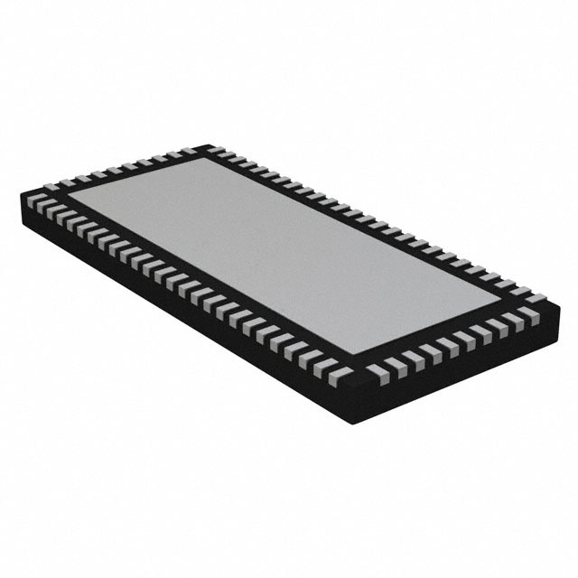
• Packaging (Pb-free & Green): 72 - Contact TQFN
Pericom Semiconductor’s PI3HDMI™ series of switch circuits
are targeted for high-resolution video networks that are based on
DVI/HDMI standards. The PI3HDMI1310-A is a 3-to-1 HDMI
Mux/DeMux Switch. It is designed for low bit-to-bit skew and
high channel-to-channel noise isolation. The maximum DVI/
HDMI data rate of 3.4Gbps provides the resolution required
by next generation HDTV and PC graphics. Three differential
channels are used for data (video signals for DVI or audio/video
signals for HDMI), and one differential channel is used for Clock
for decoding the TMDS signals at the outputs.
Block Diagram
Pin Configuration (Top View)
GND
VDD50
HPDA
HPDC
HPDB
D0-A
D0+A
D1-A
GND
DDC_CLK B
DDC_CLK
DDC_DATA
DDC_DATA B
DDC_CLK C
DDC_DATA C
HPD_A
HPD_B
HPD_Sink
HPD_C
100kΩ
VDD
D2+A
3
60
HPD_Sink
SEL1 SEL2
OE
1
GND
D3-A
4
59
SEL2
D3+A
5
58
SEL1
VDD
6
57
OE
D0-B
7
56
VDD
D0+B
8
55
D0-
D1-B
9
54
D0+
D1+B
10
53
GND
D2-B
11
52
D1-
D2+B
12
51
D1+
VDD
13
50
VDD
D3-B
14
49
D2-
D3+B
15
48
D2+
GND
16
47
GND
D0-C
17
46
D3-
D0+C
18
45
D3+
D1-C
19
44
VDD
D1+C
20
43
DDC_Data
VDD
21
42
DDC_CLK
D2-C
22
41
GND
D2+C
23
40
GND
D3-C
24
39
GND
D3+C
25
38
GND
GND
26 27 28 29 30 31 32 33 34 35 36 37
GND
GND
Control Logic
61
GND
DDC_DATA A
2
DDC_CLKC
DDC_CLK A
1 72 71 70 69 68 67 66 65 64 63 62
DDC_DataC
4 - differential�
GND
D2-A
VDD50
D0-D3±
DDC_CLKB
TMDS Lanes
DDC_DataB
4 - differential�
TMDS Lanes
TMDS Lanes
12-0196
D1+A
TMDS Lanes
4 - differential�
GND
D0-D3C±
4 - differential�
DDC_CLKA
D0-D3B±
All TMDS I/O pins are protected with Pericom's ESD protection
circuits, supporting protection against ESD damage as high as
±8kV contact per IEC6000-4-2 spec.
DDC_DataA
D0-D3A±
PI3HDMI1310-A was designed specifically to meet ATC-Sink
requirement for the HPD ports. The high speed video ports and
DDC ports can be either source or sink.
www.pericom.com 01/25/13
�PI3HDMI1310-A
HDMI™ Switch with non-blocking EQ Circuitry
Pin Description
Pin #
Pin Name
Pin Type
Description
69, 68, 71, 70,
3, 2, 5, 4,
Dx±A (X = 0, 1, 2, 3)
I/O
Port A High Speed inputs
8, 7, 10, 9, 12,
11, 15, 14
Dx±B (X = 0, 1, 2, 3)
I/O
Port B High Speed inputs
18, 17, 20, 19,
23, 22, 25, 24
Dx±C (X = 0, 1, 2, 3)
I/O
Port C High Speed inputs
65, 66, 67
HPDA, HPDB, HPDC
Output
HPD open-drain outputs for each port. Logic will follow
truth table on page 7.
External 1Kohm pull-up to 5V is required
33, 64
VDD50
Power
5.0V voltage rail from HDMI/DVI connector. Used during
standby-mode.
60
HPD_Sink
Input
GP I/O pin from SCALAR. Internal 100Kohm pull-down.
29, 28, 32, 31,
35, 34, 42, 43
DDC_CLKx, DDC_Datax
I/O
I2C signals for DDC communication on TMDS ports
55, 54, 53, 52,
51, 49, 48, 46,
45
DX± (x = 0, 1, 2, 3)
I/O
4-differential high speed Output signals
58, 59
SEL1, SEL2
Inputs
Selection for D0-D3 and DDC signals (Select Pins, see truth
tables on page 5)
6, 13, 21, 44,
50, 56, 61
VDD
Power
3.3V Power Supply
1, 16, 26, 27,
30, 36, 37, 38,
39, 40, 41, 53,
62, 63, 72
GND
Power
Ground.
57
OE
Input
Output enable (Active LOW). When HIGH, all outputs are
Hi-Z and chip is placed into Standby Mode. Under Standby
Mode, the current supply is from VDD50.
12-0196
2
www.pericom.com 01/25/13
�PI3HDMI1310-A
HDMI™ Switch with non-blocking EQ Circuitry
BLOCK DIAGRAM EXPLANATION
DDC Switch Block
Passive NMOS based 3:1 mux for DDC channels from each HDMI/DVI input connector. This section can remain active even when
3.3V supply is gone, as long as 5.0V from TMDS connector is connected to the PI3HDMI1310-A IC.
3:1 High speed Differential Channel Block
4-differential channels per port. 3 channels are targeted for high speed data channels (250Mbps to 3.4Gbps) and 1 channel is
targeted for high speed clock signal (25MHz to 340MHz).
HPD Control Channels Block
Drives each HPD channels through the input pin, HPD_Sink.
This signal will need to drive external pull-down transistor circuit before connecting to the HDMI/DVI connector. The external
pull down circuit will look like the following:
5V
1KΩ
HPD
HPDA
5V
1KΩ
HPD
HPDB
5V
1KΩ
HPDC
HPD
12-0196
3
www.pericom.com 01/25/13
�PI3HDMI1310-A
HDMI™ Switch with non-blocking EQ Circuitry
Truth table for D0-D3 and DDC Signals
SEL1
SEL2
Output Port
0
0
Port A
0
1
Port B
1
0
Port C
1
1
Hi-Z
Truth table for HPDx signals
Control Pins
Hot Plug Detect Status
OE
SEL1
SEL2
HPD_Sink HPD A
HPD B
HPD C
x
L
L
L
Hi-Z
Hi-Z
Hi-Z
x
L
L
H
L
Hi-Z
Hi-Z
x
L
H
L
Hi-Z
Hi-Z
Hi-Z
x
L
H
H
Hi-Z
L
Hi-Z
x
H
L
L
Hi-Z
Hi-Z
x
H
L
H
Hi-Z
Hi-Z
Hi-Z
L
x
H
H
L
Hi-Z
Hi-Z
Hi-Z
x
H
H
H
Hi-Z
Hi-Z
Hi-Z
*All Hi-Z will become H if external pull-up connected at the output.
Maximum Ratings
(Above which useful life may be impaired. For user guidelines, not tested.)
Storage Temperature .....................................................–65°C to +150°C
Supply Voltage to Ground Potential ................................–0.5V to +4.0V
DC Input Voltage ............................................................... –0.5V to 4.0V
DC Output Current ....................................................................... 120mA
Power Dissipation ............................................................................ 0.5W
Note: Stresses greater than those listed under MAXIMUM RATINGS may cause permanent damage to
the device. This is a stress rating only and functional
operation of the device at these or any other conditions
above those indicated in the operational sections of
this specification is not implied. Exposure to absolute
maximum rating conditions for extended periods may
affect reliability.
DC Electrical Characteristics for Switching over Operating Range (TA = –40°C to +85°C, VDD =
3.3V ±10%)
Parameter
Description
Test Conditions(1)
Min
VIH
Input HIGH Voltage
Guaranteed HIGH level
1.5
VIL
Input LOW Voltage
Guaranteed LOW level
–0.5
VIK (3)
Clamp Diode Voltage
VDD = Max., IIN = –18mA
12-0196
4
Typ(2)
–0.7
Max
Units
0.65
V
–1.2
www.pericom.com 01/25/13
�PI3HDMI1310-A
HDMI™ Switch with non-blocking EQ Circuitry
DC Electrical Characteristics for Switching over Operating Range (TA = –40°C to +85°C, VDD =
3.3V ±10%)
Parameter
Description
Test Conditions(1)
Typ(2)
IIH
Input HIGH Current
VDD = Max., VIN = VDD
±5
IIL
Input LOW Current
VDD = Max., VIN = GND
±5
IOFF
Off Leakage Current, for high
speed channels only
Vinput = 3.6V, VDD = 0V
50
Min
Max
Units
µA
Status Pins (HPD_SINK)
VIH
LVTTL Input HIGH Voltage
2
5.3
VIL
LVTTL Input LOW Voltage
GND
0.8
RP
Pull-down Resistance
VDD50 = 5.0V
V
100k
Ohm
Power Supply Characteristics
Parameters
Description
IDD
Operating Power Supply Current
IDDQ
Standby Supply Current
Test Conditions(1)
Typ.(2)
Max.
VDD = Max., VSELx = GND or
VDD
6
10
OE - High
3
5
Min.
Units
mA
Dynamic Electrical Characteristics Over the Operating Range (TA= -40º to +85ºC,
VDD = 3.3V ±10%, GND=0V)
(2)
Parameter
Description
Test Conditions
XTALK
Crosstalk on High Speed Channels
f= 1.13 GHz
See Fig. 3 for Measurement Setup
f = 825 MHz
-34
OIRR
OFF Isolation on High Speed
Channels
f= 1.13 GHz
See Fig. 2 for Measurement Setup
f = 825 MHz
-28
DR = 1.54Gbps
-1.5
DR = 2.0Gbps
Differential Insertion Loss on High
DR = 2.25Gbps
Speed Channels (see figure 1)
DR = 3.0Gbps
ILOSS
DR = 3.4Gbps
BW
-3dB BW for TMDS channels
Min
Typ.
Max
-36
Units
dB
-32
-1.73
-1.82
dB
-1.99
-2.08
3.0
GHz
Status Pins (HPD) - open drain output buffer
VOL(TTL)
TTL Low-level output voltage
IOL = 4mA
0.4
V
Notes:
1. For Max. or Min. conditions, use appropriate value specified under Electrical Characteristics for the applicable device type.
2. Typical values are at VDD = 3.3V, TA = 25°C ambient and maximum loading.
3. Substrate diode voltage drop. For testing reference.
12-0196
5
www.pericom.com 01/25/13
�PI3HDMI1310-A
HDMI™ Switch with non-blocking EQ Circuitry
Fig.1
Test Circuit
Test Circuit
Fig.2
Fig.3
12-0196
Test Circuit
6
www.pericom.com 01/25/13
�PI3HDMI1310-A
HDMI™ Switch with non-blocking EQ Circuitry
Switching Characteristics (TA= -40º to +85ºC, VDD = 3.3V±10%)
Parameter
Description
Min.
Max.
tPZH, tPZL
Line Enable Time
0.5
25
tPHZ , tPLZ
Line Disable Time
0.5
25
tb-b
Bit-to-bit skew within the same differential pair
15
tch-ch
Channel-to-channel skew
35
Units
ns
ps
Test Circuit for Electrical Characteristics(1-5)
6.0V
VDD
200-ohm
Pulse
Generator
VIN
VOUT
D.U.T
4pF
CL
RT
200-ohm
Notes:
1. CL = Load capacitance: includes jig and probe capacitance.
2. RT = Termination resistance: should be equal to ZOUT of the Pulse Generator
3. Output 1 is for an output with internal conditions such that the output is low except when disabled by the output control.
output 2 is for an output with internal conditions such that the output is high except when disabled by the output control.
4. All input impulses are supplied by generators having the following characteristics: PRR ≤ MHz, ZO = 50Ω, t R ≤ 2.5ns, t F ≤ 2.5ns.
5. The outputs are measured one at a time with one transition per measurement.
Switch Positions
Test
Switch
tPLZ , tPZL (output on B-side)
6.0V
tPHZ , tPZH (output on B-side)
GND
Prop Delay
Open
12-0196
7
www.pericom.com 01/25/13
�PI3HDMI1310-A
HDMI™ Switch with non-blocking EQ Circuitry
Packaging Mechanical: 72-Contact TQFN
Notes:
1. All dimensions are in mm. Angles in degrees.
2. Coplanarity applies to the exposed pad as well as the terminals.
3. Refer JEDEC MO-220
4. Recommended land pattern is for reference only.
5. Thermal pad soldering area.
6. Recommended thermal via diameter (drill size) is 0.3mm and via pitch is 1.27mm.
DATE: 06/10/11
DESCRIPTION: 72-contact, Very Thin Quad Flat No-Lead (TQFN)
PACKAGE CODE: ZL72
DOCUMENT CONTROL #: PD-2075
REVISION: B
11-0119
Note:
For latest package info, please check: http://www.pericom.com/products/packaging/mechanicals.php
Ordering Information
Ordering Code
Package Code
Package Description
PI3HDMI1310-AZLE
ZL
Pb-free and Green 72-contact TQFN
Notes:
• Thermal characteristics can be found on the company web site at www.pericom.com/packaging/
• "E" denotes Pb-free and Green
• Adding an "X" at the end of the ordering code denotes tape and reel packaging
12-0196
All trademarks are property of their respective owners.
8
www.pericom.com 01/25/13
�


 工商网监
湘ICP备2023018690号
工商网监
湘ICP备2023018690号
