PI3HDMI511
HDMI™1.4 Redriver Source-side Application
Features
Description
ÎÎHDMITM 1.4 compliant re-driver
PI3HDMI511 is TMDS Redriver supporting HDMI 1.4 and
DVI specifications up to a data rate of 3.4Gbps with 48-bit per
pixel Deep ColorTM. It also support enhanced robust ESD/EOS
protection of 8kV, which is required by many consumer video
networks today.
ÎÎOperation upto 3.4 Gbps per lane (340MHz pixel clock)
àà 4K x 2K 24Hz(297MHz)
àà 3D Video formats(1080p, 1080i, 720p)
ÎÎSupport up to 48-bit per pixel Deep ColorTM
ÎÎConvert low-swing DC
It converts the DC and AC coupled source devices into the
HDMI compliant signal with proper signal swing, espically in
the Notebook HDMI and Dual mode DP PC systems.
or AC coupled differential input
àà Open-drain current steering Rx terminated differential
output
àà Support Dual Mode DisplayPort source devices
Programmable termination settings at TMDS input help to
avoid the compatibility issue caused by non standard HDMI
source to determine the connection status of TMDS channel
with proper termination voltage setting.
ÎÎProvide Output Squelch function to turn off TMDS
common mode output buffer when TMDS clock is not
present
ÎÎProgrammable equalizer, emphasis and amplitude settings
With Pericom's intelligent power management techniques, the
PI3HDMI511 can automatically enter low power states when no
valid signal presents on the TMDS link.
ÎÎIntegrated Passive DDC level shifter
Pin Configuration
ÎÎBuilt-in Rx sense detection function
to achieve optimized HDMI signal integrity
àà 3.3V source to 5V sink
ÎÎ3.3V Power supply required
32 31 30 29 28
ÎÎIntegrated ESD protection on I/O pins
àà 8kV contact per IEC61000-4-2, level 4
àà 8kV HBM
ÎÎPackaging
àà Pb-free & Green
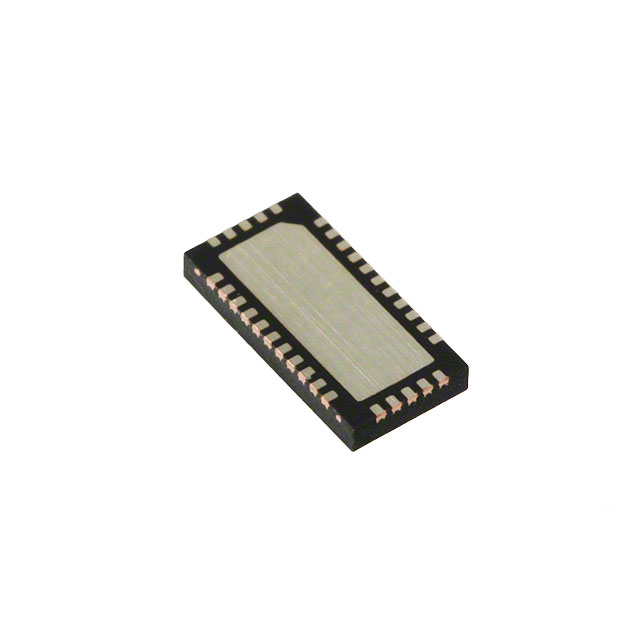
àà 32-contact TQFN (ZL)Description
Application
VDD
CEXT
1
27
SCL_SINK
2
26
OUT_D2-
IN_D2-
3
25
OUT_D2+
IN_D2+
4
OUT_D1-
IN_D1IN_D1+
5
PI3HDMI511 24
23
TQFN- 32
22
OUT_D1+
VDD
IN_D0-
7
21
OUT_D0-
IN_D0+
8
20
OUT_D0+
IN_CLK-
9
19
OUT_CLK-
18
OUT_CLK+
EQ_S0
6
IN_CLK+ 10
HPD_SRC 11
ÎÎNotebook computers and docking station
ÎÎSet-Top Box(STB)
17
12 13 14 15 16
OC_S0
1
TEST
12-0185
GND
ÎÎDongle and switch boxes
SCL_SRC
SDA_SRC
ÎÎA/V Home entertainment systems
All trademarks are property of their respective owners.
/OE
GND
GND
ÎÎProgrammable input TMDS termination control (on or off)
SDA_SINK
standby
HPD_SINK
ÎÎIdle clock detection function for output squelch and auto
www.pericom.com
P-0.2 07/10/12
�PI3HDMI511
HDMI 1.4 Redriver for Source-side Application
TM
Pin Description
Pin #
Pin Name
Type
Description
2
CEXT
PWR
LDO output for internal core supplier. External capacitor 2.2 to 4.7μF should be added to
GND.
3
IN_D2-
I
4
IN_D2+
I
5
IN_D1-
I
6
IN_D1+
I
7
IN_D0-
I
8
IN_D0+
I
9
IN_CLK-
I
10
IN_CLK+
I
11
HPD_SRC
O
HPD output; internal pull-down at 300K ohm
12
SDA_SRC
IO
DDC Data on source side
13
SCL_SRC
IO
DDC Clock on source side
15
Test
I
Must be tied LOW for normal operation
16
OC_S0
I
TMDS inputs. RT=50 ohm
TMDS output pre-emphasis selection. See OC_S0 truth table for functionality.
This pin has internal 100K ohm pull-up
TMDS input equalization selection.
If LOW or floating , EQ is set at 9dB for all TMDS data inputs
17
EQ_S0
I
If HIGH, EQ is set at 15dB for all TMDS data inputs (please note, TMDS clock inputs are
always set to 3dB EQ)
This pin has an internal 100K ohm pull-down
18
OUT_CLK+
O
19
OUT_CLK-
O
20
OUT_D0+
O
21
OUT_D0-
O
23
OUT_D1+
O
24
OUT_D1-
O
25
OUT_D2+
O
26
OUT_D2-
O
27
SCL_SINK
IO
Sink side DDC Clock
28
SDA_SINK
IO
Sink side DDC Data
29
HPD_SINK
I
Sink side hot plug detector input; internal pull-down at 120K ohm.
30
/OE
I
1, 22
VDD
PWR
14, 31, 32
GND
Ground Power Ground
All trademarks are property of their respective owners.
TMDS outputs.
Output Enable control. Active low. Internal 100K ohm pull-down. See truth table for
functionality.
3.3V power supply
12-0185
2
www.pericom.com
P-0.2 07/10/12
�PI3HDMI511
HDMI 1.4 Redriver for Source-side Application
TM
Block diagram:
CEXT
HPD_SRC
LDO
VDD
HPD_SINK
300K ohm
120K ohm
VDD
RX_CTRL
RT
RX_SENSE
RT
IN_CLK+/RXSEN
IN_Dx+/-
OUT_CLK+/-
TX
OUT_Dx+/-
Clock Detection
VDD
100K ohm
OC_S0
EQ_S0
Control Logic
/OE
100K ohm
SCL_SRC
SCL_SINK
SDA_SINK
SDA_SRC
Description of Operation
Squelch function:
Squelch control is using low frequency signal detection. When TMDS input clock frequency is less than 10MHz, it will show no
input signal. When input signal is not present, IC will enter power-down mode.
Rx-sense detector:
The PI3HDMI511 will check 50 ohm termination resistor(RT) within HDMI Rx chipset. If the RT=50 ohm is not present, we assume
no valid HDMI Rx is connected.
Therefore, IC will turn off our 50 ohm input termination resistor for all TMDS data and clock channels.When no valid RT = 50 ohm
is detected in the HDMI Receiver, the IC will enter to the power-down mode.
OC_S0 Truth Table
TMDS Output Pre-emphasis Setting
TMDS Input Equalization Setting
OC_S0
(internal
pull-up)
Single-end
Vswing (mV)
Pre-emphasis
(dB)
EQ_S0
0
500
0 (open drain)
0
1
500
2.5 (open drain)
1
Equalization
/OE
Operation
9dB
0
Normal Operation Mode
15dB
1
Power Down Mode
(dB)
Note
Note
For clock channel, pre-emphesis value is fixed to 0 dB.
For CLK channel, the EQ value is fixed to
3dB.
All trademarks are property of their respective owners.
12-0185
/OE Truth Table
3
www.pericom.com
P-0.2 07/10/12
�PI3HDMI511
HDMI 1.4 Redriver for Source-side Application
TM
Absolute Maximum Ratings
Item
Rating
Supply Voltage to Ground Potential
5.5V
All Inputs and Outputs
-0.5V to VDD+0.5V
Storage Temperature
-65 to +150°C
Junction Temperature
150°C
Soldering Temperature
260°C
Note: Stresses greater than those listed under
MAXIMUM RATINGS may cause permanent
damage to the device. This is a stress rating only
and functional operation of the device at these
or any other conditions above those indicated
in the operational sections of this specification
is not implied. Exposure to absolute maximum
rating conditions for extended periods may affect reliability.
Recommended Operation Conditions
Parameter
Min.
Ambient Operating Temperature
-40
Power Supply Voltage (measured in respect to GND)
3.0
Typ.
3.3
Max.
Unit
+85
°C
3.6
V
DC Specification
Parameter
Parameter
VDD
Operating Voltage
IDD
VDD Supply Current
Idd_Squelch
Supply Current in squelch
mode
Idd_Rx
Sense
supply current when no 50ohm
detected in Rx
Istb
Standby mode
VDD=3.6V, HPD_SINK=0, /OE =
High
VOL_HPD
Open Drain Output Low Voltage
IOL = 4 mA
IOFF_HPD
Off leakage current
IOZ_HPD
Open drain Output leakage
current
All trademarks are property of their respective owners.
Conditions
Min.
Typ.
Max.
3.3
Output Enable (open drain 500mV
single-ended 0dB pre-emphasis)
Input TMDS signal not valid,
/OE = Low
Input TMDS is valid, but 50ohm Rx
Sense(RXSEN) is not detected
Unit
V
120
150
mA
11
13
mA
4
5
mA
4
5
mA
0.4
V
/OE = Low
0
VDD=0, VIN=3.6V
20
VDD=0, VIN=5.5V
40
VDD=3.6, VIN=3.6V
20
VDD=3.6, VIN=5.5V
40
12-0185
4
www.pericom.com
µA
P-0.2 07/10/12
�PI3HDMI511
HDMI 1.4 Redriver for Source-side Application
TM
HPD_SINK
Symbol
Parameter
Conditions
Min.
IIH
High level digital input current
VIH =VDD
IIL
Low level digital input current
VIH
High level digital input voltage
VIL
Low level digital input voltage
Typ.
Max.
Units
25
40
µA
VIL = GND
-10
10
µA
VDD=3.3V
2.0
V
0
0.8
V
Max.
Units
Control Pin (/OE)
Symbol
Parameter
Conditions
Min.
Typ.
IIH
High level digital input current
VIH =VDD
30
45
µA
IIL
Low level digital input current
VIL = GND
-10
10
µA
VIH
High level digital input voltage
2.0
VIL
Low level digital input voltage
0
V
0.8
V
Max.
Units
DDC Channel Block
Symbol
Parameter
Conditions
Min.
Typ.
CIO
Input/Output capacitance
VI peak-peak = 1V, 100 KHz
10
RON
On resistance
IO = 3mA, VO = 0.4V
25
50
Ω
Vpass
Switch Output voltage
VI=3.3V, II=100uA
VDD=3.3V, External pull-up to
VDD(15K ohm ~ 5K ohm)
1.5
2.0
2.5
V
Min.
Typ.
Max.
Units
10
µA
35
50
µA
Typ.
Max.
Units
35
50
µA
10
µA
Max.
Units
pF
Control Pins(OC_S0 with 100K ohm pull-up)
Symbol
Parameter
Conditions
IIH
High level logic input current
VIH=VDD
IIL
Low level logic input current
VIL=GND
Control Pins(EQ_S0 with 100K ohm pull-down)
Symbol
Parameter
Conditions
IIH
High level logic input current
VIH=VDD
IIL
Low level logic input current
VIL=GND
Min.
TMDS Differential Pins
Symbol
Parameter
All trademarks are property of their respective owners.
Conditions
12-0185
Min.
5
Typ.
www.pericom.com
P-0.2 07/10/12
�PI3HDMI511
HDMI 1.4 Redriver for Source-side Application
TM
VOH
Single-ended high level output
voltage
VDD-10
VDD+10
VOL
Single-ended low level output
voltage
VDD-600
VDD-400 mV
Vswing
Single-ended output swing
voltage
400
600
mV
VOD(O)
Overshoot of output differential voltage (1)
180
mV
VOD(U)
Undershoot of output differential voltage (2)
200
mV
VOD(U)
Change in steady-state common-mode output voltage
between logic
5
mV
IOS
VDD = 3.3V, Rout=50 ohm
Short Circuit output current
-12
12
mV
mA
Short Circuit output current
at double termination mode
-24
24
VI(open)
Single-ended input voltage
under high impedance input
or open
II = 10uA
VDD-10
VDD+10
mV
RT
Input termination resistance
VIN = 2.9V
45
55
Ω
IOZ
Leakage current with Hi-Z I/O
VDD = 3.6V, /OE=High
10
µA
50
Note:
1. Overshoot of output differential voltage VOD(O) = (VSWING(MAX) * 2) * 15%,
2. Undershoot of output differential voltage VOD(U) = (VSWING(MIN) * 2) * 25%
All trademarks are property of their respective owners.
12-0185
6
www.pericom.com
P-0.2 07/10/12
�PI3HDMI511
HDMI 1.4 Redriver for Source-side Application
TM
AC Characteristics (Over recommended operating conditions unless otherwise noted)
TMDS Differential Pins
Symbol
Parameter
Conditions
Min.
Typ.
Max.
tpd
Propagation delay
2000
tr
Differential output signal
rise time (20% - 80%)
190
tf
Differential output signal
fall time (20% - 80%)
tsk(p)
Pulse skew
10
50
tsk(D)
Intra-pair differential skew
23
50
tsk(o)
Inter-pair differential skew
tjit(pp)
Peak-to-peak output jitter
CLK residual jitter
tjit(pp)
Peak-to-peak output jitter
DATA Residual Jitter
ten
Enable time
1000
tdis
Disable time
10
Units
ps
190
VDD = 3.3V, Rout = 50-ohm
100
Data Input = 1.65 Gbps HDMI
data pattern
CLK Input = 165 MHz clock
15
30
18
50
ps
ns
DDC I/O Pins (SCL_SRC, SCL_SINK, SDA_SRC, SDA_SINK)
Symbol
Parameter
Conditions
tpd(DDC)
Propagation Delay
CL = 10pF
Min.
Typ.
Max.
Units
0.4
2.5
ns
Typ.
Max.
Units
Control and Status Pins (HPD_SINK, HPD)
Symbol
Parameter
Conditions
tpd(HPD)
Propagation Delay
CL = 10pF, pull-up resistor=1K
ohm, Open drain output
All trademarks are property of their respective owners.
12-0185
Min.
7
10
www.pericom.com
ns
P-0.2 07/10/12
�PI3HDMI511
HDMI 1.4 Redriver for Source-side Application
TM
Packaging Mechanical: 32-Contact TQFN (ZL)
1
DATE: 10/09/09
DESCRIPTION: 32-contact, Thin Fine Pitch Quad Flat No-Lead (TQFN)
PACKAGE CODE: ZL (ZL32)
REVISION: A
DOCUMENT CONTROL #: PD-2044
09-0125
Please check for the latest package information on the Pericom web site at www.pericom.com/packaging/.
Pericom Semiconductor Corporation • 1-800-435-2336
All trademarks are property of their respective owners.
12-0185
8
www.pericom.com
P-0.2 07/10/12
�PI3HDMI511
HDMI 1.4 Redriver for Source-side Application
TM
Related DisplayPort/Dual Mode DisplayPort Products
Part Number
Product Description
Availability
PI3HDMI1201
DisplayPort 1.2 Re-driver with built-in AUX listener
Now
PI3VDP1430
Dual Mode DisplayPort to HDMI Level Shifter and Re-driver
Now
PI3HDMI611
3.4G HDMI1.4 Re-driver for Sink application, supporting Dual Mode DisplayPort
Now
PI3VDP3212
2-Lane DisplayPort1.2 Compliant Switch
Now
PI3VDP12412
4-Lane DisplayPort1.2 Compliant Switch
Now
PI3HDMI412AD
1:2 Active 3.4Gbps HDMI1.4 compliant Splitter/Re-driver
Now
PI3HDMI521
2:1 3.4Gbps HDMI1.4 Switch/Re-driver with built-in ARC and Fast Switching support
for Source Application
Now
PI3HDMI621
2:1 3.4Gbps HDMI1.4 Switch/Re-driver with built-in ARC and Fast Switching support
for Sink Application
Now
PI3HDMI336
3:1 Active 3.4Gbps HDMI Switch/Re-driver with I2C control and ARC Transmitter
Now
Reference Information
Document
Description
AN
PI3HDMI511 HDMI1.4 Application Note
VESA DisplayPort Standard Version 1 Revision 2, Video Electronics Standards Association, January 5, 2010
VESA
VESA DisplayPort Dual-Mode Standard Version 1, Video Electronics Standards Association, February 10,
2012
VESA DisplayPort Interoperability Guideline Version 1.1a, Video Electronics Standards Association, February 5, 2009
HDMI
High-Definition Multimedia Interface Specification Version 1.4, HDMI Licensing, LLC, June 5, 2009
Ordering Information
Ordering Number
Package Code
Package Description
PI3HDMI511ZLE
ZLE
Pb-free & Green 32-Contact TQFN
• Thermal characteristics can be found on the company web site at www.pericom.com/packaging/
• E = Pb-free and Green
• X suffix = Tape/Reel
All trademarks are property of their respective owners.
12-0185
9
www.pericom.com
P-0.2 07/10/12
�PI3HDMI511
HDMI 1.4 Redriver for Source-side Application
TM
Revision Histroy
Date
Changes
07/19/12
Add Tr in the block diagram, IDD,Istb with Passive DDC level shifter.
All trademarks are property of their respective owners.
12-0185
10
www.pericom.com
P-0.2 07/10/12
�PI3HDMI511
HDMI 1.4 Redriver for Source-side Application
TM
Appendix A: Generic Application Information
Eye Diagram Performance:
Figure 1: Eye Diagram at 1920x1080p 48bit Deep Color with 48” Input Trace, 9dB Equalization, 500mV Swing, 2.5dB Preemphasis.
All trademarks are property of their respective owners.
12-0185
11
www.pericom.com
P-0.2 07/10/12
�PI3HDMI511
HDMI 1.4 Redriver for Source-side Application
TM
Measurement setup:
Figure 2: Test Setup of AC-coupled TMDS Input
Figure 3: Test Setup of DC-coupled TMDS Input
All trademarks are property of their respective owners.
12-0185
12
www.pericom.com
P-0.2 07/10/12
�PI3HDMI511
HDMI 1.4 Redriver for Source-side Application
TM
Application Information:
Figure 4: Application Diagram
For more detailed application information, please refer to “PI3HDMI511_HDMI_ApplicationInformation.doc”.
All trademarks are property of their respective owners.
12-0185
13
www.pericom.com
P-0.2 07/10/12
�PI3HDMI511
HDMI 1.4 Redriver for Source-side Application
TM
Recommended Power Supply Decoupling Circuit
Figure 5 is the recommended power supply decoupling circuit configuration. It is recommended to put a 0.1μF decoupling capacitors
on each VDD pin of our part. Four 0.1μF decoupling capacitors are put in Figure 5 with an assumption of only four VDD pins on our
part.
On top of 0.1μF decoupling capacitor on each VDD pin, it is recommended to put a
10μF decoupling capacitor near our part’s VDD for stabilizing the power supply for our part. Ferrite bead is also recommended for
isolating the power supply for our part and other power supplies in other parts of the circuit. But, it is optional and depends on the
power supply conditions of other circuits.
Figure 5 Recommended Power Supply Decoupling Circuit Diagram
All trademarks are property of their respective owners.
12-0185
14
www.pericom.com
P-0.2 07/10/12
�PI3HDMI511
HDMI 1.4 Redriver for Source-side Application
TM
Requirements on the Decoupling Capacitors
i: There is no special requirement on the material of the capacitors. Ceramic capacitors are generally being used with typically
materials of X5R or X7R.
ii: 0.1uF decoupling capacitor in 0402 package is recommended.
Layout and Decoupling Capacitor Placement Consideration
i. Each 0.1μF decoupling capacitor should be placed as close as possible to each VDD pin.
ii. VDD and GND planes should be used to provide a low impedance path for power and ground.
iii. Via holes should be placed to connect to VDD and GND planes directly.
iv. The width between the traces should be as wide as possible.
v. Trace length should be as short as possible.
vi. The placement of decoupling capacitor and the way of routing trace should consider the power flowing criteria.
vii. 10μF capacitor should also be placed close to our part and should be placed in the middle location of 0.1μF capacitors.
viii. Avoid the large current circuit placed close to our part; especially when it is shared the same VDD and GND planes, since large
current flowing on our VDD or GND planes will generate a potential variation on the VDD or GND of our part.
Figure 6 Layout and Decoupling Capacitor Placement Diagram
All trademarks are property of their respective owners.
12-0185
15
www.pericom.com
P-0.2 07/10/12
�PI3HDMI511
HDMI 1.4 Redriver for Source-side Application
TM
Appendix B: Evaluation Board Schematic and Layout
5
4
3
2
1
0.1u C103
D
/OE
HPD_SINK
SDA_SINK
D
0.1u C102
4.7u C101
+3V3
+5V
27
26
25
24
23
22
21
20
19
18
17
SCL_SINK
OUT_D2+
OUT_D2OUT_D1+
OUT_D1-
J102
OUT_D0+
OUT_D0OUT_CK+
OUT_CK-
SDA_SRC
SCL_SRC
GND
Test
OC_S0
R104
2K2
R105
2K2
1
2
R103
VDD
SCL_Sink
VDD_REG
OUT_D0IN_D0OUT_D0+
IN_D0+
OUT_D1IN_D1- PI3HDMI511 OUT_D1+
IN_D1+ TQFN-32
VDD
IN_D2OUT_D2IN_D2+
OUT_D2+
IN_CLKOUT_CLKIN_CLK+
OUT_CLK+
HPD_SRC
EQ_S0
12
13
14
15
16
R102
4K7
R101
47K
+5V_A
CON_HDMI_Plug
1
2
3
4
5
6
7
8
9
10
11
JP103
2
1
1
2
JP102
JP101
+5V
2
1
20
21
C105 4.7u
IN_CK-
JP104
SCL_SINK
SDA_SINK
HPD_SINK
+5V
SDA_SRC
SCL_SRC
1
2
3
4
5
6
7
8
9
10
11
12
13
14
15
16
17
18
19
SHELL1
SHELL2
IN_D0IN_CK+
D2+
D2 SHIELD
D2D1+
D1 SHIELD
D1D0+
D0 SHIELD
D0CK+
CK SHIELD
CKCEC
NC
SCL
SDA
PGND
+5V
HPD
CON_HDMI_Recept
C
SHELL3
SHELL4
HGND
GND
GND
OE/
HPD_Sink
SDA_Sink
U101
IN_D1IN_D0+
22
23
IN_D2IN_D1+
33
32
31
30
29
28
IN_D2+
1
2
3
4
5
6
7
8
9
10
11
12
13
14
15
16
17
18
19
47K
C
J101
D2+
D2 SHIELD
D2D1+
D1 SHIELD
D1D0+
D0 SHIELD
D0CK+
CK SHIELD
CKCEC
NC
SCL
SDA
PGND
+5V
HPD
0.1u C104
SHELL1
20
+3V3
HPD_SRC
R108
R109
4K7
B
4K7
+3V3
B
External Wiring
SW101
R106
R107
4K7
4K7
1
2
3
4
/OE
Test
OC_S0
EQ_S0
8
7
6
5
SW_X4_Half_Pitch
External Wiring
D101
B0520LW
U102
REG1117-3.3V
+3V3
2
ADJ/GND
R110
R111
C110
1
VOUT
C109
VIN
+
1u
CON_USB2.0_MiniB_SMT
C108
C107
3
100u
A
+5V
+5V_USB D102
B0520LW
A
+
NP
1u
2
1
1
2
3
4
5
4.7u C106
VBUS
DD+
ID
GND
22u
JP105
+5V_A
J103
Title
0
PI3HDMI511 DEMO BOARD SCHEMATIC
Size
Date:
5
4
3
1
of
1
EDIT DATE
May 31, 2012
DOCUME
16
Rev
A
Sheet
ORIGINATE DATE
April 24, 2012
12-0185
Wednesday, April 25, 2012
1
Appendix A: PI3HDMI511 Demo Board Rev.A
Appendix B: PI3HDMI511 Demo Board Rev.A Schematic
All trademarks are property of their respective owners.
Document Number
2
www.pericom.com
P-0.2 07/10/12
�