PI3L301D
3.3V, 16-Bit to 8-Bit, Mux/DeMux
Gigabit Ethernet LAN Switch with Single Enable
Features
Description
•
•
•
•
•
•
•
•
•
•
•
Pericom Semiconductor’s PI3L series of logic circuits are produced
using the Company’s advanced sub-micron CMOS technology,
achieving industry leading performance.
RON is 4Ω typical
Low bit-to-bit skew: 200ps
Low crosstalk: –27dB @ 250MHz
Low Current Consumption: 20µA
Near-Zero propagation delay: 250ps
Switching speed: 9ns
Channel On-Capacitance: 9.5pF (typical)
VCC Operating Range: +3.0V to +3.6V
ESD >3000V . . . Human Body Model
>350 MHz bandwidth (or data frequency)
Packaging (Pb-free & Green available):
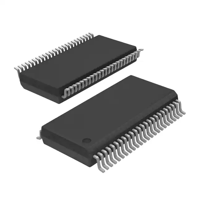
48-pin 240 mil wide plastic TSSOP (A)
The PI3L301D is a 16- to 8-bit multiplexer/demultiplexer LAN
Switch. Industry leading advantages include a propagation delay
of less than 250ps, resulting from its low channel resistance and
I/O capacitance. The device multiplexes differential outputs
from a Gigabit Ethernet transceiver (PHY) device to one of two
corresponding B1 or B2 outputs. The switch is bidirectional and
offers little or no attenuation of the high-speed signals at the outputs.
It is designed for low bit-to-bit skew, high channel-to-channel noise
isolation and is compatible with various standards, such as 10/100/
1000 Base-T (Ethernet).
Generally, this part can be used to replace mechanical relays in
low-voltage LAN applications that interface a physical layer over
CAT 5 or CAT 6 unshielded twisted pair cable through an isolation
transformer.
Applications
• Dual Physical Layer Device sharing to one interface
connector
• SONET OC-12(622Mbps) signal routing
• Routes physical layer signals for 10/100/1000 Mbit Ethernet
Pin Description
Block Diagram
A0
0B1
A1
1B1
0B2
1B2
A2
2B1
A3
3B1
3B2
A4
4B1
A5
5B1
1
48
A0
2
47
1B1
GND
3
46
GND
A1
4
45
0B2
GND
5
44
1B2
GND
V DD
6
43
GND
7
42
2B1
A2
8
41
3B1
GND
2B2
4B2
5B2
0B1
V DD
9
40
GND
A3
10
11
39
38
2B2
GND
3B2
V DD
12
37
GND
GND
13
36
V DD
NC
14
35
4B1
A4
15
34
5B1
GND
16
33
GND
A5
17
32
GND
4B2
18
31
5B2
GND
A6
6B1
V DD
19
30
A7
7B1
GND
20
29
A6
6B1
21
28
GND
7B1
22
27
A7
GND
23
24
26
6B2
6B2
7B2
SEL
SEL
13-0142
1
25
7B2
www.pericom.com PS8162F 05/08/13
�PI3L301D
3.3V, 16-Bit to 8-Bit, Mux/DeMux
Gigabit Ethernet LAN Switch with Single Enable
Maximum Ratings
Truth Table
(Above which useful life may be impaired. For user guidelines,
not tested.)
Storage Temperature....................................–65°C to +150°C
Supply Voltage to Ground Potential...............–0.5V to +4.0V
DC Input Voltage............................................–0.5V to +5.5V
DC Output Current......................................................120mA
Power Dissipation...........................................................0.5W
Function
SEL
AN to NB1
L
AN to NB2
H
Note:
Stresses greater than those listed under MAXIMUM RATINGS may cause
permanent damage to the device. This is a stress rating only and functional operation of the device at these or any other conditions above those
indicated in the operational sections of this specification is not implied.
Exposure to absolute maximum rating conditions for extended periods
may affect reliability.
13-0142
2
www.pericom.com PS8162F 05/08/13
�PI3L301D
3.3V, 16-Bit to 8-Bit, Mux/DeMux
Gigabit Ethernet LAN Switch with Single Enable
DC Electrical Characteristics for 1000 Base-T Ethernet Switching over Operating Range
(TA = –40°C to +85°C, VCC = 3.3V ±10%)
Paramenter
Test Conditions(1)
Description
Min.
Typ.(2)
Max. Units
VIH
Input HIGH Voltage
Guaranteed HIGH level
2
-
-
VIL
Input LOW Voltage
Guaranteed LOW level
–0.5
-
0.8
VIK
Clamp Diode Voltage
VCC = Max., IIN = –18mA
-
–0.7
–1.2
IIH
Input HIGH Current
VCC = Max., VIN = VCC
-
-
±5
IIL
Input LOW Current
VCC = Max., VIN = GND
-
-
±5
IOFF
Power Down Leakage Current
VCC = 0V, VA = 0V, VB ≤ 3.6
-
-
±5
RON
Switch On-Resistance(3)
VCC = Min., 1.5V ≤ VIN ≤ VCC,
IIN = –40mA
-
4
8
RFLAT(ON)
On-Resistance Flatness(4)
VCC = Min., VIN @ 1.5V and VCC,
IIN = –40mA
-
1
-
∆RON
On-Resistance match from center
ports to any other port(4)
VCC = Min., 1.5V ≤ VIN ≤ VCC,
IIN = –40mA
-
0.9
2
V
µA
Ω
DC Electrical Characteristics for 10/100 Base-T Ethernet Switching over Operating Range
(TA = –40°C to +85°C, VCC = 3.3V ±10%)
Paramenter
Test Conditions(1)
Description
Min.
Typ.(2)
Max. Units
VIH
Input HIGH Voltage
Guaranteed HIGH level
2.0
-
-
VIL
Input LOW Voltage
Guaranteed LOW level
–0.5
-
0.8
VIK
Clamp Diode Voltage
VCC = Max., IIN = –18mA
-
–0.7
–1.2
IIH
Input HIGH Current
VCC = Max., VIN = VCC
-
-
±5
IIL
Input LOW Current
VCC = Max., VIN = GND
-
-
±5
IOFF
Power Down Leakage Current
VCC = 0V, VA = 0V, VB ≤ 3.6
-
-
±5
RON
Switch On-Resistance(3)
VCC = Min., 1.25V ≤ VIN ≤ VCC,
IIN = –10mA to –30mA
-
-
8
RFLAT(ON)
On-Resistance Flatness(4)
VCC = Min., VIN @ 1.25V and VCC,
IIN = –10mA to –30mA
-
1.0
-
∆RON
On-Resistance match from center ports VCC = Min., 1.25V ≤ VIN ≤ VCC,
to any other port(4)
IIN = –10mA to –30mA
-
0.9
2.0
V
µA
Ω
Capacitance (TA = 25°C, f = 1MHz)
Parameters(4)
CIN
Description
Test Conditions
Input Capacitance
COFF(B1, B2)
Port B Capacitance, Switch OFF
CON(A/B)
A/B Capacitance, Switch ON
VIN = 0V
Typ.
Max.
3.1
3.6
2.8
6.0
9.5(5)
10.9
Units
pF
Notes:
1. For max. or min. conditions, use appropriate value specified under Electrical Characteristics for the applicable device type.
2. Typical values are at Vcc = 3.3V, Ta = 25°C ambient and maximum loading.
3. Measured by the voltage drop between A and B pins at indicated current through the switch. On-Resistance is determined by the lower of the
voltages on the two (A & B) pins.
4. This parameter is determined by device characterization but is not production tested.
5. Measured on worst case corner pin.
13-0142
3
www.pericom.com PS8162F 05/08/13
�PI3L301D
3.3V, 16-Bit to 8-Bit, Mux/DeMux
Gigabit Ethernet LAN Switch with Single Enable
Power Supply Characteristics
Parameters
ICC
Test Conditions(1)
Description
Quiescent Power Supply Current
VCC = Max., VIN = GND or VCC
Min.
Typ.(2)
Max.
Units
-
-
800
µA
Notes:
1. For max. or min. conditions, use appropriate value specified under Electrical Characteristics for the applicable device type.
2. Typical values are at Vcc = 3.3V, Ta = 25°C ambient and maximum loading.
Dynamic Electrical Characteristics Over the Operating Range (TA=-40º to +85ºC, VCC=3.3V±10%, GND=0V)
Parameter
Test Conditions(1)
Description
Min.
Typ.(2)
Max.
XTALK
Crosstalk
f = 250MHz, See Fig. 2
-
-27
-
OIRR
OFF Isolation
f = 250MHz, See Fig. 3
-
-32
-
BW
Bandwidth –3dB
CL = 10pf, See Fig. 1
-
350
-
Units
dB
MHz
Switching Characteristics
Paramenter
Test
Min.
Conditions
Description
tPD
Propagation Delay(3,4)
tPZH, tPZL
tPHZ, tPLZ
Typ.
(2)
Max.
-
0.25
Line Enable Time - SEL to AN, BN
0.5
-
15
Line Disable Time - SEL to AN, BN
0.5
-
9
tSK(o)
Output Skew between center port (A4 to A5) to any other port(4)
-
0.1
0.2
tSK(p)
Skew between opposite transitions of the same output
(tPHL - tPLH) (4)
-
0.1
0.2
Units
ns
Notes:
1. For max. or min. conditions, use appropriate value specified under Electrical Characteristics for the applicable device type.
2. Typical valves are at Vcc = 3.3V, Ta = 25°C ambient and maximum loading.
3. The bus switch contributes no propagational delay other than the RC delay of the On-Resistance of the switch and the load capacitance. The
time constant for the switch alone is of the order of 0.25ns for 10pF load. Since this time constant is much smaller than the rise/fall times of
typical driving signals, it adds very little propagational delay to the system. Propagational delay of the bus switch when used in a system is
determined by the driving circuit on the driving side of the switch and its interactions with the load on the driven side.
4. Guaranteed by design.
13-0142
4
www.pericom.com PS8162F 05/08/13
�PI3L301D
3.3V, 16-Bit to 8-Bit, Mux/DeMux
Gigabit Ethernet LAN Switch with Single Enable
Test Circuit for Electrical Characteristics
6.0V
VCC
200-ohm
Pulse
Generator
VIN
VOUT
D.U.T
10pF
CL
RT
200-ohm
Notes:
CL = Load capacitance: includes jig and probe capacitance.
RT = Termination resistance: should be equal to ZOUT of the Pulse Generator
All input impulses are supplied by generators having the following characteristics: f = 10MHz, ZO = 50Ω, tR ≤ 2.5ns, tF ≤ 2.5ns.
The outputs are measured one at a time with one transition per measurement.
Switch Positions
Test
Switch
tPLZ, tPZL (output on B-side)
6.0V
tPHZ, tPZH (output on B-side)
GND
Prop Delay
Open
HP4396B
R
S
T
HP11667A
VCC
PI3L301D
50-ohm
50-ohm
50-ohm
CL = 10pF
Figure 1. Bandwidth -3db Testing
13-0142
5
www.pericom.com PS8162F 05/08/13
�PI3L301D
3.3V, 16-Bit to 8-Bit, Mux/DeMux
Gigabit Ethernet LAN Switch with Single Enable
HP4396B
R
S
T
HP11667A
PI3L301D
50-ohm
100
-ohm
50-ohm
50-ohm
100
-ohm
Figure 2. Crosstalk Test Setup
HP4396B
R
S
T
HP11667A
50-ohm
PI3L301D
50-ohm
50-ohm
100
-ohm
Figure 3 . Off Isolation Tets Setup
13-0142
6
www.pericom.com PS8162F 05/08/13
�PI3L301D
3.3V, 16-Bit to 8-Bit, Mux/DeMux
Gigabit Ethernet LAN Switch with Single Enable
Switching Waveforms
2.5V
SEL
1.25V
1.25V
0V
Input A
3.5V
2.5V
Input
tPHL
1.5V
VDD
VOL +0.3V
tPHZ
tPZH
VOH –0.3V
VDD/2
VOH
2.5V
tPLZ
VDD/2
2.5V
tPLH
Output
tPZL
Output A
2.5V
Voltage Waveforms Propagation Delay Times
VOH
VDD/2
Output B
VOL
VOL
tPHZ
tPZH
VOL
VOL
VDD/2
VOL
Voltage Waveforms Enable and Disable Times
3.5V
Data In at
Ax or Ay
2.5V
tPLHX
1.5V
tPHLX
3.5V
VOH
2.5V
Data Out
at MBx
I
tSK(o)
tPLH
VOL
1.5V
2.5V
Output
2.5V
VOL
VOL
tPLHy
tPHL
VOH
VOH
Data Out
at MBy
2.5V
Input
tSK(p) = I tPHL – tPLH I
tPHLy
tSK(o) = I tPLHy – tPLHx I or I tPHLy – tPHLx I
Output Skew - tSK(o)
Pulse Skew - tSK(p)
Applications Information
Logic Inputs
The logic control inputs can be driven up to +3.6V regardless of the supply voltage. For example, given a +3.3V supply, the output
enables or select pins may be driven low to 0V and high to 3.6V. Driving IN Rail-to-Rail® minimizes power consumption.
Power-Supply Sequencing
Proper power-supply sequencing is advised for all CMOS devices. It is recommended to always apply VCC before applying signals to
the input/output or control pins.
Rail-to-Rail is a registered trademark of Nippon Motorola, Ltd
13-0142
7
www.pericom.com PS8162F 05/08/13
�PI3L301D
3.3V, 16-Bit to 8-Bit, Mux/DeMux
Gigabit Ethernet LAN Switch with Single Enable
Packaging Mechanical: 48-Pin TSSOP (A)
DOCUMENT CONTROL NO.
PD - 1501
48
REVISION: G
DATE: 03/09/05
.236
.244
6.0
6.2
See Note 4
1
.488 12.4
.496 12.6
See Note 3
.047
1.20 Max
SEATING PLANE
1
.004 0.09
.008 0.20
X.XX
X.XX
DENOTES DIMENSIONS
IN MILLIMETERS
.002
.006
0.05
0.15
.007
.010
.0197
BSC
0.50
0.17
0.27
Note:
1. Controlling dimensions in millimeters.
2. Ref: JEDEC MO-153F/ED
3. Dimension does not include mold flash, protrusions or gate burrs. Mold flash, protrusions and gate burrs shall not exceed 0.15mm per side.
4. Dimension does not include interlead flash or protrusion. Interlead flash or protrusion
shall not exceed 0.25mm per side.
0.45 .018
0.75 .030
.319
BSC
8.1
Pericom Semiconductor Corporation
3545 N. 1st Street, San Jose, CA 95134
1-800-435-2335 • www.pericom.com
DESCRIPTION: 48-Pin 240-Mil Wide TSSOP
PACKAGE CODE: A
Ordering Information
Ordering Code
PI3L301DAE
Package Code
Package Description
A
Pb-free & Green, 48-pin 240 mil wide plastic TSSOP
Notes:
• Thermal characteristics can be found on the company web site at www.pericom.com/packaging/
• E = Pb-free & Green
• Adding an X suffix = Tape/Reel
13-0142
8
www.pericom.com PS8162F 05/08/13
�


 工商网监
湘ICP备2023018690号
工商网监
湘ICP备2023018690号
