PI3L500-A
3.3V, 8-Channel, 2:1 Mux/DeMux
Gigabit Ethernet LAN Switch with Single Enable
and Enhanced ESD Protection
Features
Description
•
•
•
•
•
•
•
•
•
RON is 4Ω typical
Low bit-to-bit skew: 200ps
Low Crosstalk: –35dB @ 250MHz
Near-Zero propagation delay: 250ps
Switching speed: 9ns
Channel On capacitance: 10pF (typical)
Status Indicator LEDs Switched with Ethernet pairs
VCC Operating Range: +3.0V to +3.6V
Enhanced ESD Protection:
– 8kV (contact)(1)
– Switch pins: 1.1kV (machine model),
12kV (human body model)
• >550 MHz bandwidth (or data frequency)
• Packaging:
– Pb-free and Green, 56-contact TQFN (ZF)
The PI3L500-A is a 8-Channel 2:1 multiplexer/demultiplexer LAN
Switch with Hi-Z outputs. Industry leading advantages include a
propagation delay of less than 250ps, resulting from its low channel
resistance and I/O capacitance. The device multiplexes differential
outputs from a Gigabit Ethernet transceiver (PHY) device to one
of two corresponding B1 or B2 outputs. The switch is bidirectional
and offers little or no attenuation of the high-speed signals at the
outputs. It is designed for low bit-to-bit skew, high channel-tochannel noise isolation and is compatible with various standards,
such as 10/100/1000 Base-T (Ethernet).
Generally, this part can be used to replace mechanical relays in
low-voltage LAN applications that interface a physical layer over
CAT 5 or CAT 6 unshielded twisted pair cable through an isolation
transformer.
Note: 1. IEC 61000-4-2
Applications
• Dual Physical Layer Device sharing to one interface
connector
• Routes signals for 10/100/1000 Mbit Ethernet
10-0178
1
GND
2LED1
2LED2
VCC
GND
51
50
49
LED2
52
GND
54
53
VCC
2 B1
7
42
3 B1
8
41
2 B2
9
40
3 B2
10
39
11
38
GND
VCC
12
37
4 B1
13
36
5 B1
14
35
4 B2
15
34
16
33
5 B2
17
32
18
31
19
30
20
29
28
43
GND
SEL
GND
6
27
XLED2
44
26
XLED1
1 B2
5
VCC
LEDX
45
1LED2
7B2
0 B2
4
25
6B2
46
0LED2
7B1
1 B1
3
24
A7
6B1
0 B1
47
GND
A6
48
2
23
1B2
1
1LED1
GND
A0
A1
VCC
N.C.
GND
A2
A3
GND
VCC
A4
A5
GND
A6
A7
GND
SEL
VCC
LED0
LED1
0B2
55
1B1
22
A1
21
0B1
GND
A0
56
Pin Description
0LED1
Block Diagram
GND
6 B1
7 B1
6 B2
7 B2
PS8803A
06/08/10
�PI3L500-A
3.3V, 8-Channel, 2:1 Mux/DeMux Gigabit Ethenet LAN
Switch w/Single Enable and Enhanced ESD Protection
Pin Description
Truth Table
Pin Name
Description
AX
DeMux Inputs
XBY
Mux Inputs
LEDZ
LED Demux Inputs
ZLEDY
LED Mux Inputs
GND
Ground
VCC
Power
SEL
Select
SEL
Function
L
AX to XB1; LEDZ to ZLED1
H
AX to XB2; LEDZ to ZLED2
Maximum Ratings
(Above which useful life may be impaired. For user guidelines, not tested.)
Storage Temperature......................................................... –65°C to +150°C
Supply Voltage to Ground Potential
............................ –0.5V to +4.0V
DC Input Voltage................................................................. –0.5V to +5.5V
DC Output Current........................................................................... 120mA
Power Dissipation............................................................................... 0.5W
Note:
Stresses greater than those listed under MAXIMUM RATINGS may cause permanent
damage to the device. This is a stress rating only and functional operation of the device
at these or any other conditions above those indicated in the operational sections of this
specification is not implied. Exposure to absolute maximum rating conditions for extended
periods may affect reliability.
10-0178
2
PS8803A
06/08/10
�PI3L500-A
3.3V, 8-Channel, 2:1 Mux/DeMux Gigabit Ethenet LAN
Switch w/Single Enable and Enhanced ESD Protection
DC Electrical Characteristics for 1000 Base-T Ethernet Switching over Operating Range
(TA = –40°C to +85°C, VCC = 3.3V ±10%)
Paramenter
Description
Test Conditions(1)
Min.
Typ.(2)
Max.
VIH
Input HIGH Voltage
Guaranteed HIGH level (Control Pins)
2.0
–
–
VIL
Input LOW Voltage
Guaranteed LOW level (Control Pins)
–0.5
–
0.8
VIK
Clamp Diode Voltage
VCC = Max., IIN = –18mA
–
–0.7
–1.2
IIH
Input HIGH Current
VCC = Max., VIN = VCC
–
–
±5
IIL
Input LOW Current
VCC = Max., VIN = GND
–
–
±5
RON
Switch On-Resistance(3)
VCC = Min., 1.5V ≤ VIN ≤ VCC
IIN = –40mA
–
4.0
6.5
RFLAT(ON)
On-Resistance Flatness(3)
VCC = Min., VIN @ 1.5V and VCC
IIN = –40mA
–
0.5
–
ΔRON
On-Resistance match from center VCC = Min., 1.5V ≤ VIN ≤ VCC
ports to any other port(3)
IIN = –40mA
–
0.4
1.0
Units
V
µA
Ω
DC Electrical Characteristics for 10/100 Base-T Ethernet Switching over Operating Range
(TA = –40°C to +85°C, VCC = 3.3V ±10%)
Paramenter
Description
Test Conditions(1)
Min.
Typ.(2)
Max.
VIH
Input HIGH Voltage
Guaranteed HIGH level (Control Pins)
2.0
–
–
VIL
Input LOW Voltage
Guaranteed LOW level (Control Pins)
–0.5
–
0.8
VIK
Clamp Diode Voltage
VCC = Max., IIN = –18mA
–
–0.7
–1.2
IIH
Input HIGH Current
VCC = Max., VIN = VCC
–
–
±5
IIL
Input LOW Current
VCC = Max., VIN = GND
–
–
±5
RON
Switch On-Resistance(3)
VCC = Min., 1.25V ≤ VIN ≤ VCC IIN =
–10mA to –30mA
–
4.0
6.5
RFLAT(ON)
On-Resistance Flatness(3)
VCC = Min., VIN @ 1.25V and VCC IIN
= –10mA to –30mA
–
0.5
–
∆RON
On-Resistance match from cen- VCC = Min., 1.25V ≤ VIN ≤ VCC IIN =
ter ports to any other port(3)
–10mA to –30mA
–
0.4
1.0
Capacitance (TA = 25°C, f = 1MHz)
Parameters(4)
Description
CIN
Input Capacitance
COFF(B1, B2)
Port B Capacitance, Switch OFF
CON(A/B)
A/B Capacitance, Switch ON
Test Conditions(1)
VIN = 0V
Typ.
Max.
2.0
3.0
4.0
6.0
10.0
11.0
Units
V
µA
Ω
Units
pF
Notes:
1. For max. or min. conditions, use appropriate value specified under Electrical Characteristics for the applicable device type.
2. Typical values are at Vcc = 3.3V, Ta = 25°C ambient and maximum loading.
3. Measured by the voltage drop between A and B pins at indicated current through the switch. ON resistance is determined by the lower of the
voltages on the two (A & B) pins.
4. This parameter is determined by device characterization but is not production tested.
10-0178
3
PS8803A
06/08/10
�PI3L500-A
3.3V, 8-Channel, 2:1 Mux/DeMux Gigabit Ethenet LAN
Switch w/Single Enable and Enhanced ESD Protection
Power Supply Characteristics
Parameters
ICC
Test Conditions(1)
Description
Quiescent Power Supply Current
VCC = Max., VIN = GND or VCC
Min.
Typ.(2)
Max.
Units
—
0.5
3.5
mA
Dynamic Electrical Characteristics Over the Operating Range (TA = –40°C to +85°C,
Parameter
Test Conditions(1)
Description
XTALK
Crosstalk(3)
OIRR
OFF
RL = 100Ω, f = 250MHz
Isolation(3)
Bandwidth –3dB(3)
BW
RL = 100Ω
Vcc = 3.3V ±10%, GND = 0V)
Min.
Typ.(2)
Max.
—
–35
—
—
–32
—
—
350
—
MHz
Max.
Units
Units
dB
Switching Characteristics
Min.
Typ.(2)
tPD
Propagation
Delay(3,4)
–
0.25
tPZH, tPZL
Line Enable Time - SEL to AN, BN
0.5
–
15.0
tPHZ, tPLZ
Line Disable Time - SEL to AN, BN
0.5
–
9.0
tSK(o)
Output Skew between center port (A4 to A5) to any other
–
0.1
0.2
tSK(p)
Skew between opposite transitions of the same output (tPHL - tPLH
–
0.1
0.2
Paramenter
Description
port(3)
) (3)
ns
Notes:
1. For max. or min. conditions, use appropriate value specified under Electrical Characteristics for the applicable device type.
2. Typical values are at Vcc = 3.3V, Ta = 25°C ambient and maximum loading..
3. Guaranteed by design.
4. The bus switch contributes no propagational delay other than the RC delay of the ON resistance of the switch and the load capacitance. The
time constant for the switch alone is of the order of 0.25ns for 10pF load. Since this time constant is much smaller than the rise/fall times of
typical driving signals, it adds very little propagational delay to the system. Propagational delay of the bus switch when used in a system is
determined by the driving circuit on the driving side of the switch and its interactions with the load on the driven side.
10-0178
4
PS8803A
06/08/10
�PI3L500-A
3.3V, 8-Channel, 2:1 Mux/DeMux Gigabit Ethenet LAN
Switch w/Single Enable and Enhanced ESD Protection
Test Circuit for Electrical Characteristics
6.0V
VCC
Switch Positions
200-ohm
Pulse
Generator
VIN
Test
VOUT
D.U.T
10pF
CL
RT
200-ohm
Switch
tPLZ, tPZL (output on B-side)
6.0V
tPHZ, tPZH (output on B-side)
GND
Prop Delay
Open
Notes:
CL = Load capacitance: includes jig and probe capacitance.
RT = Termination resistance: should be equal to ZOUT of the Pulse Generator
Test Circuit for Dynamic Electrical Characteristics
S1
HP4195A
VCC
T1
D.U.T
HP11667A
10-0178
R1
10pF
5
50-ohm
PS8803A
06/08/10
�PI3L500-A
3.3V, 8-Channel, 2:1 Mux/DeMux Gigabit Ethenet LAN
Switch w/Single Enable and Enhanced ESD Protection
Switching Waveforms
2.5V
SEL
2.5V
Input
0V
2.5V
tPLH
tPHL
1.5V
Output
2.5V
tPZL
tPLZ
VOH
VDD/2
VOH
Output
1.25V
1.25V
3.5V
tPZH
2.5V
VOL
VOL +0.3V
tPHZ
VOH –0.3V
VDD/2
VOL
VOH
VOL
Output
Voltage Waveforms Enable and Disable Times
Voltage Waveforms Propagation Delay Times
3.5V
2.5V
Data In
tPLHX
1.5V
tPHLX
3.5V
VOH
Data Out
at Channel X
I
tSK(o)
tPLH
VOL
VOH
2.5V
Output
VOL
VOL
tPLHy
1.5V
tPHL
VOH
2.5V
Data Out
at Channel Y
2.5V
Input
2.5V
tSK(p) = I tPHL – tPLH I
tPHLy
tSK(o) = I tPLHy – tPLHx I or I tPHLy – tPHLx I
Pulse Skew - tSK(p)
Output Skew - tSK(o)
Notes:
Waveform 1 is for an output with internal conditions such that the output is low except when disabled by the output control.
Waveform 2 is for an output with internal conditions such that the output is high except when disabled by the output control.
All input impulses are supplied by generators having the following characteristics: PRR ≤ MHz, ZO = 50Ω, tR ≤ 2.5ns, tF ≤ 2.5ns.
The outputs are measured one at a time with one transition per measurement.
Applications Information
Logic Inputs
The logic control inputs can be driven up to +3.6V regardless of the supply voltage. For example, given a +3.3V supply, the output
enables or select pins may be driven low to 0V and high to 3.6V. Driving IN Rail-to-Rail® minimizes power consumption.
Power-Supply Sequencing
Proper power-supply sequencing is advised for all CMOS devices. It is recommended to always apply VCC before applying signals to
the input/output or control pins.
Rail-to-Rail is a registered trademark of Nippon Motorola, Ltd
10-0178
6
PS8803A
06/08/10
�PI3L500-A
3.3V, 8-Channel, 2:1 Mux/DeMux Gigabit Ethenet LAN
Switch w/Single Enable and Enhanced ESD Protection
Packaging Mechanical: 56-Contact TQFN (ZF)
Ordering Information
Ordering Number
Package Code
Package Description
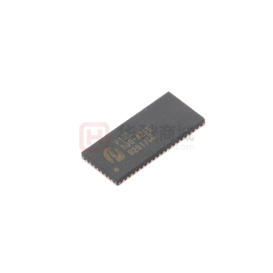
PI3L500-AZFE
ZF
Pb-free & Green, 56-contact TQFN
Notes:
Thermal characteristics can be found on the company web site at www.pericom.com/packaging/
Add 'X' for Tape and Reel
Pericom Semiconductor Corporation • 1-800-435-2336 • www.pericom.com
10-0178
7
PS8803A
06/08/10
�