PI3LVD512
3.3V, 5-differential Channel LVDS
Switch Targeted for 24bit Displays
Features
Description
•
•
•
•
•
•
Pericom’s PI3LVD512 is a 5-differential channel LVDS mux/
demux used to switch between multiple LVDS sources or end
points. In a notebook application where analog video signals
are found in both the notebook and the dock, a switch solution
is required to switch between the two video port locations. With
the high bandwidth of 870MHz, the signal integrity will remain
strong even through the long FR4 trace between the notebook and
the docking station. In addition to high signal performance, the
video signals are also protected against high ESD with integrated
diodes to VDD and GND that will support up to 12kV of ESD
HBM protection.
Designed specifically to switch LVDS signals
VDD = 3.3V +/-10%
ESD tolerance on video I/O pins is up to 12kV HBM
-3dB BW of 870MHz (typ)
Low Xtalk, (-28dB typ)
Low and Flat ON-STATE resistance (Ron = 3ohm, Ron(Flat)
= 0.5ohm, typ)
• Low input/output capacitance (Con = 6pF, typ)
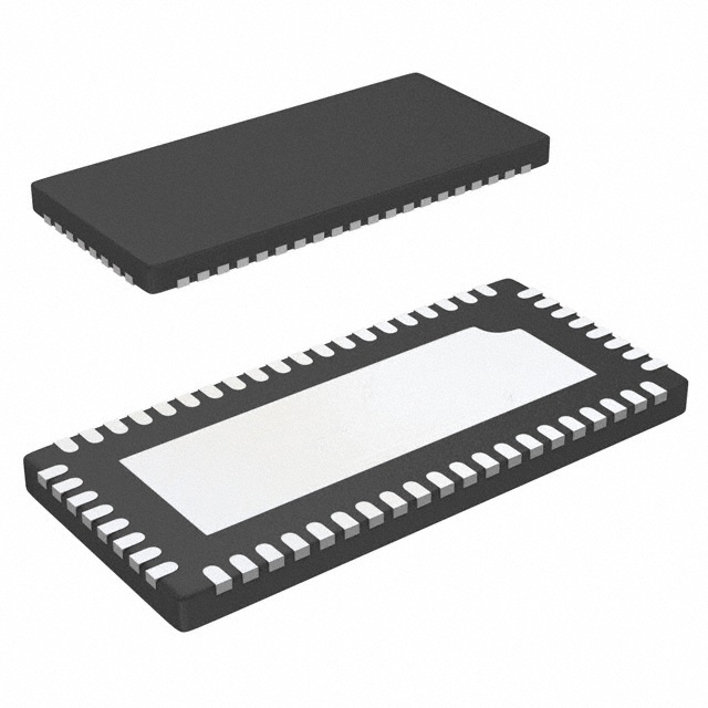
• Packaging (Pb-free and Green):
− 56 contact TQFN (ZFE)
− 42 contact TQFN (ZHE)
Applications
• Routes physical layer signals for high bandwidth
0B1
A1
1B1
0B2
GND
A0
A1
1B2
2B1
A2
3B1
A3
A4
A5
2B2
VDD
NC
3B2
GND
4B1
A2
A3
5B1
GND
VDD
4B2
A4
A5
5B2
A6
6B1
GND
A7
7B1
A6
A7
6B2
GND
7B2
A8
8B1
A9
9B1
SEL
VDD
A8
A9
8B2
NC
A0
GND
NC
NC
VDD
GND
Pin Description (56ZFE, top view)
VDD
GND
Block Diagram
56 55 54 53 52 51 50 49
1
48
2
47
3
46
4
45
5
44
43
6
7
42
8
41
40
9
39
10
38
11
37
12
36
13
35
14
34
15
33
16
32
17
18
31
19
30
20
29
21 22 23 24 25 26 27 28
0B1
1B1
0B2
1B2
GND
2B1
3B1
2B2
3B2
GND
VDD
4B1
5B1
4B2
5B2
GND
6B1
7B1
6B2
7B2
SEL
10-0185
1
GND
8B2
9B2
VDD
GND
GND
8B1
9B1
9B2
PS8979B
09/16/10
�PI3LVD512
3.3V, 5-differential channel LVDS
switch targeted for 24bit displays
A4
A5
A6
A7
SEL
VDD
A8
A9
8B1
NC
NC
VDD
0B1
40
39
18
19
20
21
9B2
VDD
41
8B2
A2
A3
42
NC
VDD
1
2
3
4
5
6
7
8
9
10
11
12
13
14
15
16
17
9b1
VDD
A0
A1
NC
Pin Description (42ZHE, top view)
38
37
36
35
34
33
32
31
30
29
28
27
26
25
24
23
22
1B1
0B2
1B2
2B1
3B1
2B2
3B2
VDD
4B1
5B1
4B2
5B2
6B1
7B1
6B2
7B2
VDD
Note:
NC pin (5) could be left floating or tied to GND
10-0185
2
PS8979B
09/16/10
�PI3LVD512
3.3V, 5-differential channel LVDS
switch targeted for 24bit displays
Maximum Ratings
(Above which useful life may be impaired. For user guidelines,
not tested.)
Note:
Stresses greater than those listed under MAXIMUM RATINGS may cause
permanent damage to the device. This is a stress rating only and functional operation of the device at these or any other conditions above those
indicated in the operational sections of this specification is not implied.
Exposure to absolute maximum rating conditions for extended periods
may affect reliability.
Storage Temperature....................................–65°C to +150°C
Supply Voltage to Ground Potential...............–0.5V to +4.0V
DC Input Voltage............................................–0.5V to +5.5V
DC Output Current......................................................120mA
Power Dissipation...........................................................0.5W
Truth Table
Input SEL
Input/Output An
Function
L
nB1
An = nB1
nB2 high impedance mode
H
nB2
An = nB2
nB1 high impedance mode
DC Electrical Characteristics for Video Switching over Operating Range
(TA = –40°C to +85°C, VDD = 3.3V ±10%)
Paramenter
Description
Test Conditions(1)
Min.
Typ.(2)
Max.
VIH
Input HIGH Voltage
Guaranteed HIGH level
2
-
-
VIL
Input LOW Voltage
Guaranteed LOW level
–0.5
-
0.8
VIK
Clamp Diode Voltage
VDD = Max., ISEL = –18mA
-
–0.7
–1.2
IIH
Input HIGH Current
VDD = Max., VSEL = VDD
-
-
±5
IIL
Input LOW Current
VDD = Max., VSEL = GND
-
-
±5
IOFF
Power Down Leakage Current
VDD = 0V, VA ≤ 3.6
-
-
±5
RON
Switch On-Resistance(3)
VDD = Min., 0.9V ≤ Vinput ≤ 1.6V,
Iinput = –40mA
-
2.8
3.5
RFLAT(ON)
On-Resistance Flatness(4)
VDD = Min., Vinput @ 0V and 1.5V,
Iinput = –40mA
-
0.5
-
∆RON
On-Resistance match from center
ports to any other port(4)
VDD = Min., 0.9V ≤ Vinput ≤ 1.6V,
Iinput = –40mA
-
0.9
2
10-0185
3
PS8979B
Units
V
µA
Ω
09/16/10
�PI3LVD512
3.3V, 5-differential channel LVDS
switch targeted for 24bit displays
Capacitance (TA = 25°C, f = 1MHz)
Parameters(4)
Test Conditions(1)
Description
CIN
Input Capacitance
COFF
Port A/B Capacitance, Switch OFF
CON
Switch Capacitance, Switch ON
Typ.(2)
Units
2.7
VSEL = 0V
2
pF
6
Notes:
1. For max. or min. conditions, use appropriate value specified under Electrical Characteristics for the applicable device type.
2. Typical values are at VDD = 3.3V, Ta = 25°C ambient and maximum loading.
3. Measured by the voltage drop between A and B pins at indicated current through the switch. On-Resistance is determined by the lower of the
voltages on the two (A & B) pins.
4. This parameter is determined by device characterization but is not production tested.
Power Supply Characteristics
Parameters
ICC
Test Conditions(1)
Description
Quiescent Power Supply Current
Min.
Typ.(2)
Max.
Units
-
-
500
µA
VDD = Max., VSEL = GND or VDD
Notes:
1. For max. or min. conditions, use appropriate value specified under Electrical Characteristics for the applicable device type.
2. Typical values are at VDD = 3.3V, Ta = 25°C ambient and maximum loading.
Dynamic Electrical Characteristics Over the Operating Range (TA=-40º to +85ºC, VDD=3.3V±10%, GND=0V)
Parameter
Description
Test Conditions
Min.
Typ.(2)
Max.
Units
XTALK
Crosstalk
f = 250MHz, See Fig. 2
-
-28
-
OIRR
OFF Isolation
f = 250MHz, See Fig. 3
-
-41
-
BW
Bandwidth –3dB
See Fig. 1
-
880
-
MHz
Min.
Typ.(2)
Max.
Units
-
0.25
ns
Switching Characteristics
Paramenter
Description
tPD
Propagation Delay(2,3)
tPZH, tPZL
Line Enable Time - SEL to Input, Output
0.5
-
15
tPHZ, tPLZ
tb-b (2)
Line Disable Time - SEL to Input, Output
0.5
-
9
-
-
15
-
-
60
tch-ch (2)
Differential Bit-to-bit Skew
Differential channel to channel skew
dB
ps
Notes:
1. For max. or min. conditions, use appropriate value specified under Electrical Characteristics for the applicable device type.
2. Guaranteed by design.
3. The switch contributes no propagational delay other than the RC delay of the On-Resistance of the switch and the load capacitance. The time
constant for the switch alone is of the order of 0.25ns for 10pF load. Since this time constant is much smaller than the rise/fall times of typical
driving signals, it adds very little propagational delay to the system. Propagational delay of the bus switch when used in a system is determined
by the driving circuit on the driving side of the switch and its interactions with the load on the driven side.
10-0185
4
PS8979B
09/16/10
�PI3LVD512
3.3V, 5-differential channel LVDS
switch targeted for 24bit displays
Test Circuit for Electrical Characteristics(1)
6.0V
VDD
200-ohm
VIN
Pulse
Generator
VOUT
D.U.T
10pF
CL
RT
200-ohm
Notes:
1. CL = Load capacitance: includes jig and probe capacitance.
2. RT = Termination resistance: should be equal to ZOUT of the Pulse Generator
3. All input impulses are supplied by generators having the following characteristics: f = 10 MHz, ZO = 50Ω, tR ≤ 2.5ns, tF ≤ 2.5ns.
4. The outputs are measured one at a time with one transition per measurement.
Switch Positions
Test
Switch
tPLZ, tPZL (output on I-side)
6.0V
tPHZ, tPZH (output on I-side)
GND
Prop Delay
Open
Test Circuit for Dynamic Electrical Characteristics
HP4396B
R
S
T
HP11667A
50-ohm
PI3LVD512
50-ohm
50-ohm
CL = See Graph Fig 4
Figure 1. Bandwidth -3dB Testing
10-0185
5
PS8979B
09/16/10
�PI3LVD512
3.3V, 5-differential channel LVDS
switch targeted for 24bit displays
HP4396B
R
S
T
HP11667A
PI3LVD512
50
100
50
50
100
Figure 2. Crosstalk Test Setup
HP4396B
R
S
T
HP11667A
50
PI3LVD512
50
50
100
Figure 3. Off Isolation Test Setup
10-0185
6
PS8979B
09/16/10
�PI3LVD512
3.3V, 5-differential channel LVDS
switch targeted for 24bit displays
Switching Waveforms
2.5V
SEL
3.5V
2.5V
Input
Output
0V
2.5V
tPLH
tPHL
1.5V
Output
tPZL
tPLZ
VDD/2
VOH
2.5V
1.25V
1.25V
VOL
VOL +0.3V
tPHZ
tPZH
2.5V
VOH
VDD/2
VOH –0.3V
VOH
VOL
Output
Voltage Waveforms Propagation Delay Times
VOL
Voltage Waveforms Enable and Disable Times
Applications Information
Logic Inputs
The logic control inputs can be driven up to +3.6V regardless of the supply voltage. For example, given a +3.3V supply, the output
enables or select pins may be driven low to 0V and high to 3.6V. Driving IN Rail-to-Rail® minimizes power consumption.
Rail-to-Rail is a registered trademark of Nippon Motorola, Ltd
10-0185
7
PS8979B
09/16/10
�PI3LVD512
3.3V, 5-differential channel LVDS
switch targeted for 24bit displays
Packaging Mechanical: 56-Pin TQFN (ZF)
1
DATE: 05/15/08
DESCRIPTION: 56-contact, Thin Fine Pitch Quad Flat No-lead (TQFN)
PACKAGE CODE: ZF56
DOCUMENT CONTROL #: PD-2024
REVISION: C
08-0208
10-0185
8
PS8979B
09/16/10
�PI3LVD512
3.3V, 5-differential channel LVDS
switch targeted for 24bit displays
Packaging Mechanical: 42 pin TQFN (ZH)
1
DATE: 02/17/09
Notes:
1. All dimensions are in millimeters, angles in degrees.
2. Coplanarity applies to the exposed thermal pad as well as the terminals.
3. Refer JEDEC MO-220
4. Recommended Land Pattern is for reference only.
5. Thermal Pad Soldering Area
DESCRIPTION: 42-contact Thin Fine Pitch Quad Flat No-Lead (TQFN)
PACKAGE CODE: ZH (ZH42)
DOCUMENT CONTROL #: PD-2035
REVISION: C
09-0116
Ordering Information
Ordering Code
Package Code
Package Description
PI3LVD512ZFE
ZFE
Pb-free & Green, 56-pin TQFN
PI3LVD512ZHE
ZHE
Pb-free and Green, 42-pin TQFN
Notes:
• Thermal characteristics can be found on the company web site at www.pericom.com/packaging/
• E = Pb-free and Green
• Adding X suffix = Tape/Reel
Pericom Semiconductor Corporation • 1-800-435-2336 • www.pericom.com
10-0185
9
PS8979B
09/16/10
�