PI3PCIE3422
3.3V, PCI Express® 3.0 2-Lane, (4-Channel), Differential Mux/Demux with Bypass
Features
Description
ÎÎ8 Differential Channel SPST switch with Mux/DeMux option
Pericom semiconductor’s PI3PCIE3422 is an 8 to 4 channel
differential multiplexer/demultiplexer featuring 8-channel passthrough. It supports two full PCIe® lanes at 8.0Gbps PCIe® 3.0
performance.
ÎÎPCIe® 3.0 performance
ÎÎBi-directional operation
ÎÎLow Bit-to-Bit Skew: 10ps (between ± signals)
ÎÎLow Crosstalk: -50dB @ 4.0GHz (8Gbps)
ÎÎLow Off Isolation:
With the select control input low Port A connects to Port B, and
Port C connects to port D for an 8-channel differential passthough. When the select control input is high Port A connects
to Port D, and Port B and Port C are in a high-impedance state.
The mux/demux function is between Port A and Ports B or D as
determined by the select input control.
-21dB @4GHz
ÎÎLow Insertion Loss: -1.8dB @ 4.0GHz (8Gbps)
ÎÎReturn Loss:
-15dB @4GHz
ÎÎVDD Operating Range: 3.3V ±10%
ÎÎESD Tolerance: 2kV HBM
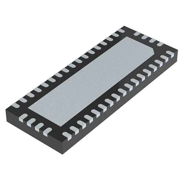
ÎÎPackaging (Pb-free & Green): 42-contact, TQFN (ZH42)
Truth Table
C0+
C0-
A1+
A1C1+
C1-
A2+
A2C2+
C2-
A3+
A3C3+
C3-
All trademarks are property of their respective owners.
D0+
D0B1+
B1-
D1+
D1B2+
B2-
D2+
D2B3+
B3-
VDD
GND
C0+
3
36
D0+
C0-
4
35
D0-
A1+
5
34
B1+
A1-
6
33
B1-
C1+
7
32
D1+
31
D1-
30
VDD
40
B0-
39
B0+
37
C1-
8
SEL
9
A2+
10
29
B2+
A2-
11
28
B2-
C2+
12
27
D2+
C2-
13
26
D2-
A3+
14
25
B3+
A3-
15
24
B3-
C3+
16
23
D3+
C3-
17
22
D3-
GND
VDD
A0+
A0-
B0+
B0-
38
2
21
OE#
SEL
1
A0-
20
Block Diagram
A0+
VDD
1
VDD
x
OE#
0
GND
Ax, Bx, Cx, Dx = Hi-Z (disconnected)
H
Pin Diagram (Top-side view)
41
B = C = Hi-Z
0
42
Ax = Dx
L
19
Cx = Dx
OE#
GND
Ax = Bx
SEL
18
Function
D3+
D3-
13-0011
1
www.pericom.com
P-0.3
12/12/12
�PI3PCIE3422
3.3V, PCI Express® 3.0 2-Lane, Differential Mux/Demux with Bypass
Pin Description
Pin #
Pin Name I/O
Description
1
A0+
I/O
Signal I/O, Channel 0, Port A
2
A0–
5
A1+
I/O
Signal I/O, Channel 1, Port A
6
A1–
10
A2+
I/O
Signal I/O, Channel 2, Port A
11
A2–
14
A3+
I/O
Signal I/O, Channel 3, Port A
15
A3–
38
B0+
I/O
Signal I/O, Channel 0, Port B
37
B0−
34
B1+
I/O
Signal I/O, Channel 1, Port B
33
B1−
29
B2+
I/O
Signal I/O, Channel 2, Port B
28
B2−
25
B3+
I/O
Signal I/O, Channel 3, Port B
24
B3−
3
C0+
I/O
Signal I/O, Channel 0, Port C
4
C0–
7
C1+
I/O
Signal I/O, Channel 1, Port C
8
C1–
12
C2+
I/O
Signal I/O, Channel 2, Port C
13
C2–
16
C3+
I/O
Signal I/O, Channel 3, Port C
17
C3−
36
D0+
I/O
Signal I/O, Channel 0, Port D
35
D0−
32
D1+
I/O
Signal I/O, Channel 1, Port D
31
D1−
27
D2+
I/O
Signal I/O, Channel 2, Port D
26
D2−
23
D3+
I/O
Signal I/O, Channel 3, Port D
22
D3−
41
OE#
I
Output Enable, active low. When OE# = 0 the device I/O is enabled. When OE#=1,
all I/O are high impedance
9
SEL
I
Operation mode Select
(when SEL=0: A→B, C→D, when SEL=1: A→D, B + C = Hi-Z)
18, 20, 30, 40, 42
VDD
Pwr
3.3V ±10% Positive Supply Voltage
19, 21, 39, Center Pad
GND
Pwr
Power ground
All trademarks are property of their respective owners.
13-0011
2
www.pericom.com
P-0.3
12/12/12
�PI3PCIE3422
3.3V, PCI Express® 3.0 2-Lane, Differential Mux/Demux with Bypass
Maximum Ratings
(Above which useful life may be impaired. For user guidelines, not tested.)
Storage Temperature .....................................................–65°C to +150°C
Supply Voltage to Ground Potential ................................–0.5V to +4.6V
Channel DC Input Voltage ................................................. –0.5V to 1.5V
DC Output Current ....................................................................... 120mA
Power Dissipation ............................................................................ 0.5W
SEL DC Input Voltage ....................................................... –0.5V to 4.6V
Note: Stresses greater than those listed under MAXIMUM
RATINGS may cause permanent damage to the device. This
is a stress rating only and functional operation of the device
at these or any other conditions above those indicated in the
operational sections of this specification is not implied. Exposure to absolute maximum rating conditions for extended
periods may affect reliability.
Electrical Characteristics Recommended Operating Conditions
Symbol
Parameter
Conditions
VDD
3.3V Power Supply
IDD
Total current from VDD
3.3V supply
TCASE
Case temperature range
for operation within spec.
Min
Typ
Max
Units
3.0
3.3
3.6
V
0.15
1
mA
85
Celsius
Max
Units
SEL and OE# at OV or VDD
-40
DC Electrical Characteristics for Switching over Operating Range
Parameters
Description
Test Conditions(1)
Min
VIH - SEL
Input HIGH Voltage, SEL input
Guaranteed HIGH level
2
3.6
VIL - SEL
Input LOW Voltage, SEL input
Guaranteed LOW level
0
0.8
VIK
Clamp Diode Voltage
VDD = Max., VIN = –18mA
IIH
Input HIGH Current for OE#
and SEL
VDD = Max., VIN = VDD
-10
10
IIH
Input HIGH Current
VDD = Max., VIN = 1.5V
-10
+10
IIL
Input LOW Current
VDD = Max., VIN = GND
-10
+10
RON
On Channel Resistance
CON
On Channel Capacitance
VDD = 3.3V, VIN = 0
IOZ
Output Current
VDD = Max., VIN = 0V to 1.5V
Typ(1)
–0.7
VDD = Min., VIN = 1.3V,
8
IIN = 40mA
V
–1.2
µA
15
Ohm
2.5
-10
pF
+10
µA
Note:
1.
Typical values are at VDD = 3.3V, TA = 25°C ambient and maximum loading.
Switching Characteristics
Parameters
Description
tPZH, tPZL
Min.
Typ.
Max.
Line Enable Time - SEL to AN, BN, CN, DN
0.5
15
25
tPHZ , tPLZ
Line Disable Time - SEL to AN, BN, CN, DN
0.5
5
25
tb-b
Bit-to-bit skew within the same differential pair
4
10
tch-ch
Channel-to-channel skew
All trademarks are property of their respective owners.
Test Conditions
13-0011
ns
ps
20
3
www.pericom.com
Units
P-0.3
12/12/12
�PI3PCIE3422
3.3V, PCI Express® 3.0 2-Lane, Differential Mux/Demux with Bypass
Dynamic Electrical Characteristics
Parameter
Description
BW
Bandwidth -3dB
Test Conditions
(VIN = -10dBm, DC = 0V)
DDILOFF
DDRL
Differential Off Isolation
Differential Return Loss
DDNEXT
Typ.(1)
Max.
7
Differential Insertion Loss
DDIL
Min.
Near End Crosstalk
Units
GHz
f=1.25GHz
-0.9
-1.0
f=2.5GHz
-1.2
-1.3
f=4.0GHz
-1.7
-1.8
f=5.0GHz
-2.0
-2.1
f=8.0GHz
-5.0
-5.1
f= 4.0GHz
-19
f= 0 to 1.25GHz
-16
-15
f= 1.25 to 2.5GHz
-15
-14
f= 2.5 to 4.0GHz
-15
-14
f= 0 to 2.8GHz
-52
f= 2.8 to 5.0GHz
-50
f= 5.0 to 8.0GHz
-48
dB
dB
dB
dB
Notes:
1.
Guaranteed by design. Typical values are at V DD = 3.3V , TA = 25°C ambient and maximum loading.
All trademarks are property of their respective owners.
13-0011
4
www.pericom.com
P-0.3
12/12/12
�PI3PCIE3422
3.3V, PCI Express® 3.0 2-Lane, Differential Mux/Demux with Bypass
Differential Insertion Loss
Differential Return Loss
All trademarks are property of their respective owners.
13-0011
5
www.pericom.com
P-0.3
12/12/12
�PI3PCIE3422
3.3V, PCI Express® 3.0 2-Lane, Differential Mux/Demux with Bypass
Differential Off Isolation
Differential Crosstalk
All trademarks are property of their respective owners.
13-0011
6
www.pericom.com
P-0.3
12/12/12
�PI3PCIE3422
3.3V, PCI Express® 3.0 2-Lane, Differential Mux/Demux with Bypass
8.0 Gbps RX signal eye without PI3PCIE3422
+
BALANCED
PORT1
–
8.0 Gbps RX signal eye with PI3PCIE3422
BALANCED
PORT1
+
BALANCED
– PORT2
+
+
50
–
–
50
+
–
DUT
BALANCED
PORT2
DUT
Differential Insertion Loss and Return Test Circuit
BALANCED
PORT1
BALANCED
PORT2
+
+ 50
–
– 50
+
+ 50
–
– 50
Differential Off Isolation Test Circuit
DUT
Differential Near End Xtalk Test Circuit
All trademarks are property of their respective owners.
13-0011
7
www.pericom.com
P-0.3
12/12/12
�PI3PCIE3422
3.3V, PCI Express® 3.0 2-Lane, Differential Mux/Demux with Bypass
Test Circuit for Electrical Characteristics(1-5)
3.0V
VDD
200-ohm
Pulse
Generator
VIN
D.U.T
VOUT
4pF
CL
RT
200-ohm
Notes:
1.
CL = Load capacitance: includes jig and probe capacitance.
2.
RT = Termination resistance: should be equal to ZOUT of the Pulse Generator
3.
Output 1 is for an output with internal conditions such that the output is low except when disabled by the output control.
output 2 is for an output with internal conditions such that the output is high except when disabled by the output control.
4.
All input impulses are supplied by generators having the following characteristics: PRR ≤ MHz, ZO = 50Ω, tR ≤ 2.5ns, tF ≤ 2.5ns.
5.
The outputs are measured one at a time with one transition per measurement.
Switch Positions
Test
Switch
tPLZ , tPZL
3.0V
tPHZ , tPZH
GND
Prop Delay
Open
Switching Waveforms
SEL
VDD/2
VDD/2
VDD
0V
Output 1
tPZL
tPLZ
0.75V
VOH
VOL + 0.15V
tPHZ
tPZH
VOH - 0.15V
0.75V
VOL
VOH
VOL
Output 2
Voltage Waveforms Enable and Disable Times
All trademarks are property of their respective owners.
13-0011
8
www.pericom.com
P-0.3
12/12/12
�PI3PCIE3422
3.3V, PCI Express® 3.0 2-Lane, Differential Mux/Demux with Bypass
Packaging Information
Notes:
1. All dimensions are in millimeters. Angles in degrees.
2. Coplanarity applies to the exposed pad as well as the terminals.
3. Refer JEDEC MO-220.
4. Recommended land pattern is for reference only.
5. Thermal pad soldering area
DATE: 11/14/12
DESCRIPTION: 42-contact Thin Fine Pitch Quad Flat No-Lead (TQFN)
PACKAGE CODE: ZH42
DOCUMENT CONTROL #: PD-2035
REVISION:D
12-0529
Note:
For latest package info, please check: http://www.pericom.com/products/packaging/mechanicals.php
Ordering Information
Ordering Code
Package Code
Package Description
PI3PCIE3422ZHE
ZH
Pb-free & Green, 42-contact TQFN
Notes:
•
Thermal characteristics can be found on the company web site at www.pericom.com/packaging/
•
"E" denotes Pb-free and Green
•
Adding an "X" at the end of the ordering code denotes tape and reel packaging
All trademarks are property of their respective owners.
13-0011
9
www.pericom.com
P-0.3
12/12/12
�