PI3TB212
10.3Gbps Thunderbolt™ and DisplayPort™ Switch
Features
Description
ÎÎSupports 5.4Gbps for DisplayPort 1.2 and 10.3Gbps for
Pericom Semiconductor's PI3TB212 is a high-speed multiplexer/demultiplexer switch. PI3TB212 can switch signals up
to 10.3125Gbps for DisplayPort and Thunderbolt™(TB) applications. The device supports 5.4Gbps for DisplayPort and
10.3125Gbps for Thunderbolt.
Thunderbolt Electrical Standard
ÎÎSupports DP and DP++ Configuration
ÎÎSupports AUX and DDC MUX
ÎÎVDD Operating Range for normal operation: 3.3V±10%
ÎÎExtended operation down to 2.5V min on the LSTx/LSRx
PI3TB212 is a major advance over first-generation Thunderbolt
solutions. PI3TB212 integrates the 10.3125 Gbps Thunderbolt
path. This eliminates external PIN diode switches, thereby
reducing board space, reducing cost, and improving link performance.
to TBC-9/TBC-11 channels (performance not guaranteed,
but all buffers will still operate)
ÎÎESD protection on all pins
ÎÎ1.0kV HBM per JESD22 standard
ÎÎ Packaging (Pb-free & Green):
PI3TB212 achieves excellent signal integrity at 10.3125 Gbps as
evidenced by measured results.
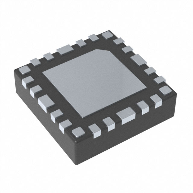
àà 3.0 mm x 3.0 mm, 24-contact TQFN
Application
Block Diagram
ÎÎThunderbolt over mini-DP connector enablement
VDD
DDC_SCL
DDC_SDA
AUX-
1
AUX+
2
VDD
TBC-16
GND
TBC-11
TBC-9
TBC-4
24
R1
TBC-18
S0
Pin Configuration (Top View)
23
22
21
20
19
18
3
TBC-16
AUX-
TBC-18
TB Rx_1(p)
R2
TB Rx_1(n)
17 TBC-2
ML1(p)
ML1(n)
16 CA_DET_Out
GND
AUX+
VDD
TBC-9
TBC-11
R3
LSTx
LSRx
15 10G_EN
GND
R4
10
11
All trademarks are property of their respective owners.
DP_EN#
10G_EN
Controller
Chip
PU/PD
Enables
12
CA_DET_Out
HPD_Out
9
ML1(p)
8
ML1(n)
7
GND
DP_EN#
6
S0
13 LSRx
5
TB_Rx_1(p)
DDC_SCL
14 LSTx
4
TB_Rx_1(n)
DDC_SDA
13-0026
TBC-4
HPD_SINK
HPD_Out
1
TBC-2
03/12/13
�PI3TB212
10.3Gbps Thunderbolt™ and DisplayPort™ Switch
Pin Description
Pin #
Pin Name
Type
Description
17
TBC-2
I
Connector Side Hot Plug Detect Input. Connect to mini-DP connector pin2
11
ML1(p)
ML1(n)
I/O
Controller Side Channel 1, DisplayPort Positive Signal (external AC coupling is required)
Controller Side Channel 1, DisplayPort Negative Signal (external AC coupling is required)
TBC-16
TBC-18
I/O
Sink Side TB Rx1(p) or AUX+ Signal or DDC_SCL. Connect to mini-DP connector pin 16.
Sink Side TB Rx1(n) or AUX- Signal or DDC_SDA. Connect to mini-DP connector pin 18.
TBC-9
TBC-11
I/O
Sink Side DP Main Link + Signal or LSTX. Connect to mini-DP connector pin 9.
Sink Side DP Main Link - Signal or LSRX. Connect to mini-DP connector pin 11
AUX+
AUX-
I/O
Controller Side AUX Positive Signal
Controller Side AUX Negative Signal
TB Rx_1(p)
TB Rx_1(n)
I/O
4
DDC_SCL
DDC_SDA
I/O
Controller Side DDC Clock
Controller Side DDC Data
18
TBC-4
I
Connector Side Cable Detect for DP++ Dongle. Connect to mini-DP connector pin 4.
12
HPD_Out
O
Controller Side Buffered Hot Plug Detect Output
14
I/O
13
LSTx
LSRx
O
Controller Side un-buffered UART TX Signal. Integrated 9KW pull-up
Controller Side buffered UART RX Signal. 1MW pull-down present at buffer input
24
S0
I
Control signal. See truth table for detailed functionality
16
CA_DET_Out
O
Cable detect buffered output coming from TBC-4 (pin 18)
6
DP_EN#
I
DisplayPort path enable. See truth table for detailed functionality.
15
10G_EN
I
10G path enable. See truth table for detailed functionality.
3
VDD
Power
3.3V+/-10% power supply voltage
Center
Pad, 9, 21
GND
Ground Ground. both pins and center pad must all be connected to GND plane.
10
22
23
19
20
2
1
8
7
5
All trademarks are property of their respective owners.
Controller Side 10Gbps Positive Signal (external AC coupling is required)
Controller Side 10Gbps Negative Signal (external AC coupling is required)
13-0026
2
03/12/13
�PI3TB212
10.3Gbps Thunderbolt™ and DisplayPort™ Switch
Description of Operation
Truth Table
Control Pins
Device and PU/PD Configurations
LSRx, HPD_Out,
& CA_DET_Out
Device States
Thunderbolt 10G mode
DisplayPort Mode
S0
10G_EN
DP_EN#
TBC-4
2:1 Mux
3:1 Mux
1 (System Active)
1
1
X
LSTx & LSRx
TB Rx_1
0 (System Sleep)
1
1
X
LSTx & LSRx
Hi-z
1 (System Active)
0
0
0
DP ML1 (p, n)
AUX
buffers
All buffers on
All buffers on
R1, R2 status
R1 = R2 = OFF
R1 = R2 = OFF
R1 = R2 = ON
0 (System Sleep)
0
0
0
Hi-Z
Hi-z
1 (System Active)
0
0
1
DP ML1 (p, n)
DDC
0 (System Sleep)
0
0
1
Hi-Z
Hi-z
Detect Mode
X - don't care
0
1
X
LSTx & LSRx
Hi-z
All buffers on
R1 = R2 = ON
Chip Disable mode
X - don't care
1
0
x
hi-z
hi-z
All buffers on
R1 = ON, R2 = ON
Power off (VDD = 0V)
X - don't care
x
x
x
hi-z
hi-z
All buffers oFF
R1 = OFF, R2 = ON
TMDS Mode
All buffers on
TBC-16
DDC_SCL or AUX(p) or TB RX_1 (p)
TBC-18
DDC_SDA or AUX(n) or TB Rx_1 (n)
TBC-9
ML1 (p) or LSTx
TBC-11
ML1 (n) or LSRx
TBC-4
CA_DET_Out
TBC-2
HPD_Out
13-0026
R1 = R2 = ON
R1 = R2 = ON
Controller Pin Names
ThunderBolt Connector Pins
All trademarks are property of their respective owners.
R1 = R2 = ON
3
03/12/13
�PI3TB212
10.3125Gbps Thunderbolt and DisplayPort Switch
Maximum Ratings
(Above which useful life may be impaired. For user guidelines, not tested.) Note: Stresses greater than those listed under MAXIMUM
Storage Temperature .....................................................–65°C to +150°C
Supply Voltage to Ground Potential .................................–0.5V to +4.6V
I/O (Pin7 and 8) DC Input Voltage .................................... –0.5V to 1.5V
I/O (pin 1, 2, 4, and 5) ........................................................-0.5V to 4.0V
I/O (pin 10 and 11)..............................................................-0.5V to 2.6V
I/O (pin 19 and 20) ............................................................. –0.5V to 4.0V
DC Output Current ........................................................................ 120mA
Power Dissipation ............................................................................ 0.5W
Control Logic DC Input Voltage .......................................... VDD + 0.5V
RATINGS may cause permanent damage to the device. This
is a stress rating only and functional operation of the device
at these or any other conditions above those indicated in the
operational sections of this specification is not implied. Exposure to absolute maximum rating conditions for extended
periods may affect reliability.
Electrical Characteristics
Recommended Operating Conditions
Symbol
Parameter
Conditions
Min
Typ
Max Units
3.0
3.3
3.6
780
VDD
3.3V Power Supply
IDD
current consumption in normal opperation
Control pins = GND or VDD, LSTx = VDD
300
Current consumption when S0 = 0
S0 = 0, TBC-2 and TBC-4 = GND or VDD,
LSTx = VDD, all I/Os are floating
100
300
IDD_detect
Current consumption during detect
S0 = VDD, 10G_EN = 0, DP_EN# = VDD,
LSTx = VDD, all I/Os are floating
120
300
PDD
Total Power from VDD 3.3V supply Control pins = GND or VDD, LSTx = VDD
IDDQ (System off)
PDDQ (Sys-
V
uA
1
2.8
mW
Power consumption when S0 = 0
S0 = 0, TBC-2 and TBC-4 = GND or VDD,
LSTx = VDD
330
1080
uW
PDD_Detect
Power consumption during detect
S0 = VDD, 10G_EN = 0, DP_EN# = VDD,
LSTx = VDD
400
1080
uW
TCASE
Case operating temperature range
105
C
tem off)
0
DC Electrical Characteristics for Switching over Operating Range
Test Conditions(1)
Parameters
Description
VIH
Input HIGH Voltage for S0, DP_EN#,
VDD = 3.3V
10G_EN, TBC-4, TBC-2, TBC-11
VIL
Input LOW Voltage for S0, DP_EN#,
10G_EN, TBC-4, TBC-2, TBC-11
VDD = 3.3V
VIK
Clamp Diode Voltage
VDD= Max., IIN = –18mA
IIH
Input HIGH Current for S0, DP_
EN#, 10G_EN, TBC-4. TBC-2
VDD = Max., VIN = VDD
IIL
Input LOW Current for S0, DP_EN#,
VDD = Max., VIN = 0V
10G_EN, TBC-4, TBC-2
VDD = 0V, 1.5V present on TBC-16
leakage from TBC-16
IOFF (TBC pins)
TB Rx_1 (p/n) is floating
VDD = 0V, 1.5V present on TBC-18
leakage from TBC-18
TB Rx_1 (p/n) is floating
leakage from TBC-9, TBC-11, TBC4, & TBC-2
All trademarks are property of their respective owners.
13-0026
VDD = 0V, 3.3V present on TBC
pins
Min
Typ(1)
Max
1.8
0.8
–0.7
-1
V
–1.2
1
µA
-1
1
-60
+60
-20
+20
-20
+20
µA
ML1(p/n) is floating
4
03/12/13
�PI3TB212
10.3125Gbps Thunderbolt and DisplayPort Switch
DC Electrical Characteristics for Switching over Operating Range
Test Conditions(1)
Typ(1)
Max
Thunderbolt 10G Mode
VDD = 3.6V. TB path on. Vin = 1.0V,
TBRx_1 (p/n) is floating
20
50
I/O leakage for DDC/AUX
VDD = 3.6V. Vin = 0V
10
15
I/O leakage for TB Rx1(p/n)
VDD = 3.6V. Vin = 0V; TBC16, 18 = 0.2V
20
50
I/O leakage for ML1
VDD = 3.6V. Vin = 0V; TBC9, 11 = 0.5V
10
15
I/O leakage for LSTx
VDD = 3.6V. Vin = 0V
-400
-300
I/O leakage for TBC9 and 11
VDD = 3.6V, Vin = 0V, ML1 (p/n) is floating
10
15
I/O leakage for TBC16 and 18
VDD = 3.6V, Vin = 0V, S0=low, 10G_EN
= high, DP_EN# = high, TBRx_1 (p/n) is
floating, Thunderbolt Mode
40
78
I/O leakage for DDC/AUX
VDD = 3.6V. Vin = VDD
10
15
I/O leakage for TB Rx1(p/n)
VDD = 3.6V. Vin = 0.5V
20
50
I/O leakage for ML1
VDD = 3.6V. Vin = 2.6V
10
15
I/O leakage for LSTx
VDD = 3.6V. Vin = VDD
10
15
I/O leakage for TBC9 and 11
VDD = 3.6V, Vin = VDD, ML1(p/n) is
floating
10
15
I/O leakage for TBC16 and 18
VDD = 3.6V, Vin = VDD, S0=low, 10G_
EN = high, DP_EN# = high, TBRx_1
(p/n) is floating, Thunderbolt mode
80
150
Parameters Description
ILeakage
IOZL
IOZH
Leakage on TB-16/TB-18
Min
-600
Units
µA
RON Table
Parameters
Description
Test Conditions
Min.
Typ.
Max. Units
RON AUX/LSTx AUX & LSTx On Resistance
VDD = 3.3V Vinput = 3.3V, Iinput = -40mA
9
15
RON TB
TB On Resistance
VDD = 3.3V Vinput = 0V, Iinput = -40mA
5
8
RON DP
DP On Resistance
VDD = 3.3V Vinput = 0V, Iinput = -40mA
5
8
RON DDC
DDC On Resistance
VDD = 3.3V Vinput = 3.3V, Iinput = -40mA
5
25
All trademarks are property of their respective owners.
13-0026
5
Ohms
03/12/13
�PI3TB212
10.3125Gbps Thunderbolt and DisplayPort Switch
Dynamic Electrical Characteristics
Description
Test Conditions
DDIL (2)
Insertion Loss on TB Rx_1 (p, n) to TBC16 and TBC-18 path
f=4.0GHz
-1.2
f=5.0GHz
-1.5
(VIN = -10dBm, DC = 0V)
f=8.0GHz
-3.0
Insertion Loss on ML1 (p, n) to TBC-9 and
TBC-11 path
f=810MHz (RBR)
-0.5
f=1.35GHz (HBR1)
-0.7
(VIN = -10dBm, DC = 0V)
f=2.7GHz (HBR2)
-1.1
f= 4.0GHz
-24
f= 5.0GHz
-16
f= 8.0GHz
-9
f= 1.35GHz
-31
f= 2.7GHz
-27
f= 6.0GHz
-17
f = 810MHz
-27
f = 1.35GHz
-22
f = 2.7GHz
-16
f = 4.0GHz
-16
f = 5.0GHz
-15
(TB RX_1)
DDIL
(ML1)
DDRL (2)
Differential Return Loss on
(TB Rx_1)
10G thunderbolt path
DDRL
Differential Return Loss on
(ML1)
DP path
Off-isolation for DP path
Off-Isolation3
Off-isolatoin for TB path
Min.
Typ.(1)
Parameter
Max.
Units
dB
dB
dB
dB
dB
dB
Notes:
1. Guaranteed by design. Typical values are at VDD = 3.3V , TA = 25°C ambient and maximum loading.
2. Refer to figure 1 for test setup
3. Refer to figure 3 for test setup
Buffers (HPD_Out, CA_DET_Out, TBC-2, TBC-4 and LSRx)
Parameters
Description
VIH
Input high for TBC-2, TBC-4
VDD = 3.6V
and TBC-11
VIL
Input Low for TBC-2, TBC-4
VDD = 3.6V
and TBC-11
VOH
Output high for HPD_Out,
CA_DET_Out, and LSRx
VDD = 3.3V+/-10%, Ioh = -2mA
VOL
Output Low for HPD_Out,
CA_DET_Out and LSRx
VDD = 3.6V, Iol = 2mA
All trademarks are property of their respective owners.
Test Conditions
13-0026
Min.
Typ.
Max.
Units
1.8
0.8
V
6
2.4
VDD
0.8
03/12/13
�PI3TB212
10.3125Gbps Thunderbolt and DisplayPort Switch
Timing
Parameter
Description
Test Conditions
Tsw
Switching time between paths
VDD = 3.0V
Tstartup
VDD valid to channel enable
Twakeup
From sleep mode to on mode (toggling S0)
VDD = 3.0V
Tb-b
Bit-to-bit skew within the same
differential pair
VDD =
3.0V
Min.
Typ.(1) Max.
VDD valid = 2.7V
VDD ramp is from 0V to 3.3V
Units
2
us
10
us
2
us
(between pin 22 & 23)
2
5
(between pin 19 & 20)
2
5
ps
Linear region for Analog switches (non-buffered paths)
Parameter
Description
Test Conditions
Min.
Typ
Max.
Units
Vp_TBT
TB Rx_1(p) and TB Rx_1(n) path (2)
VDD = 3.3V, Ipass =
10mA
1.0
1.3
V
Vp_AUX/DDC
AUX+, AUX-, DDC_SCL, & DDC_SDA
path (2)
VDD = 3.3V, Ipass =
10mA
3.6
4.2
V
Vp_ML
ML1(p) and ML1(n) path (2)
VDD = 3.3V, Ipass =
10mA
2.2
2.5
V
Vp_LSTx
LSTx signal path (2)
VDD = 3.3V, Ipass =
10mA
3.6
4.2
V
Pull-up/Pull-downs
Parameter
Description
Test Conditions
R2
Pull-down value on AUX+
path
R1
Pull-up value on AUX- path
R4
Pull-down value on LSRx
path
Min.
S0 = 10G_EN = DP_EN#=TBC-4 = 0V
VDD=3.3V, TBC-16 = 3.3V
VDD = 0V, TBC-16 = 3.3V
S0 = 10G_EN = DP_EN#=TBC-4 = 0V
VDD = 3.3V, TBC-18 = 0V
Typ.(1)
Max. Units
88
105
88
105
88
105
Kohm
Kohm
S0 = 10G_EN = 0V;
DP_EN#=TBC-11=3.3V;
1
1.5
Mohm
VDD = 3.3V
S0 = 10G_EN = 0V;
R3
Pull-up value on LSTx path
DP_EN# = VDD; LSTx=0V
8.8
10.5
Kohm
VDD = 3.3V
Notes:
1. Typical values are at VDD = 3.3V , TA = 25°C ambient and maximum loading.
2. See figure 2 for test setup
All trademarks are property of their respective owners.
13-0026
7
03/12/13
�PI3TB212
10.3125Gbps Thunderbolt and DisplayPort Switch
VDD
+
BALANCED
PORT1
+
BALANCED
PORT1
–
+
+
50
–
–
50
BALANCED
– PORT2
+
–
DUT
BALANCED
PORT2
DUT
Fig 1: Diff. Insertion Loss
and Return Test Circuit
Fig 2: Linear Region Test Setup
Fig 3: Diff. Off Isolation Test Circuit
Test Circuit for Electrical Characteristics(1-5)
VDD
Port1
Port2
D.U.T
COM Port
4pF
CL
xEN
200-ohm
Pulse
Generator
Notes:
1. CL = Load capacitance: includes jig and probe capacitance.
2. RT = Termination resistance: should be equal to ZOUT of the Pulse Generator
3. Output 1 is for an output with internal conditions such that the output is low except when disabled by the output control.
output 2 is for an output with internal conditions such that the output is high except when disabled by the output control.
4. All input impulses are supplied by generators having the following characteristics: PRR ≤ MHz, ZO = 50Ω, tR ≤ 2.5ns, tF ≤ 2.5ns.
5. The outputs are measured one at a time with one transition per measurement.
Switching Waveforms
xEN
VDD
50%
50%
0V
Output 1
Tsw
Tsw
VOH
50%
VOL
Tsw
Tsw
VOH
50%
VOL
Output 2
Test Condition:
Voltage Waveforms SwitchingTimes
Output1: Port 1=Low, Port 2=High
Output2: Port 1=High, Port 2=Low
All trademarks are property of their respective owners.
13-0026
8
03/12/13
�PI3TB212
10.3125Gbps Thunderbolt and DisplayPort Switch
Measured Insertion loss for 10Gbps Thunderbolt Path at VDD = 3.3V , TA = 25°C
Measured Return loss for 10Gbps Thunderbolt Path at VDD = 3.3V , TA = 25°C
All trademarks are property of their respective owners.
13-0026
9
03/12/13
�PI3TB212
10.3125Gbps Thunderbolt and DisplayPort Switch
Measured Data Eye for 10.3125 Gbps Thunderbolt Path at VDD = 3.0V , TA = 25°C, PRBS2^7-1
Measured Data Eye for 5.4 Gbps Display Port Path at VDD = 3.0V , TA = 25°C, PRBS2^7-1
All trademarks are property of their respective owners.
13-0026
10
03/12/13
�PI3TB212
10.3Gbps Thunderbolt™ and DisplayPort™ Switch
Packaging Mechanical: 24-Contact TQFN
DATE: 05/07/12
Notes:
1. All dimensions are in mm.
2. Coplanarity applies to the exposed thermal pad as well as the terminals
3. Refer JEDEC MO-220
DESCRIPTION: 24-contact, Very Thin Quad Flat No-Lead (TQFN)
PACKAGE CODE: ZL24
DOCUMENT CONTROL #: PD-2109
REVISION: --
Please check for the latest package information on the Pericom web site at www.pericom.com/packaging/
12-0353
Ordering Information
Ordering Number
Package Code
Package Description
PI3TB212ZLE
ZL
Pb-free & Green 24-Contact TQFN
• Thermal characteristics can be found on the company web site at www.pericom.com/packaging/
• E = Pb-free and Green
• X suffix = Tape/Reel
Pericom Semiconductor Corporation • 1-800-435-2336
All trademarks are property of their respective owners.
13-0026
11
03/12/13
�