COMPANY CONFIDENTIAL
PI3VDP1431
PI3VDP1413A
Low Power Dual-mode DisplayPort 3.4Gb/s Level Shifter/Redriver
Application
Features
ÎÎDual-mode DisplayPort level shifter/Redriver
ÎÎNotebook and Desktop computers
ÎÎOperation up to 3.4 Gbps per lane (340MHz pixel clock)
ÎÎ4K Ultra HD, 3D video formats (1080p, 1080i, 720p), 48-bit
Device Information
per pixel Deep Color support
ÎÎLow standby current with DDC passive Switch or Buffer
mode
ÎÎFlexible 3 steps equalization control steps: 2.5, 5, 7.5 dB
ÎÎPre-emphasis control 3 steps: 0, 1.5, 2.5 dB
Part Number
Package/Body Size Description
PI3VDP1431
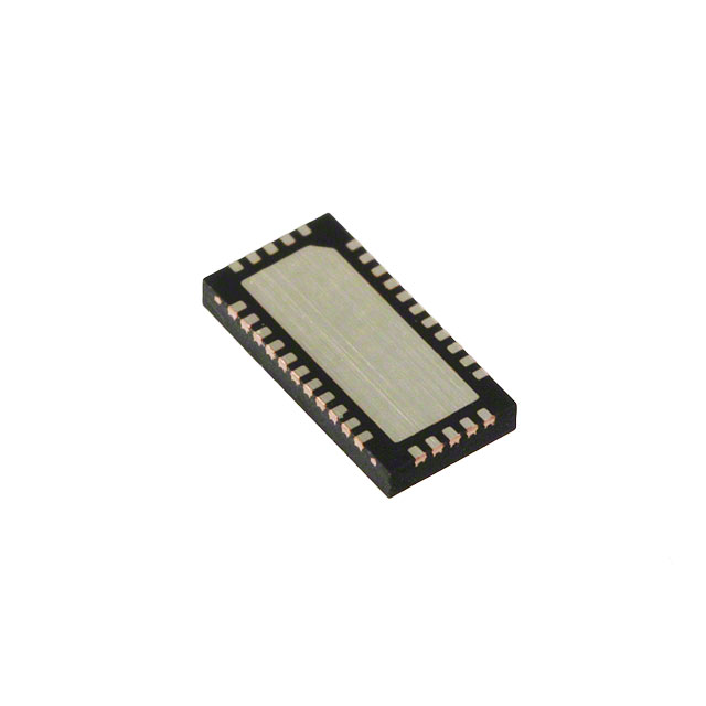
TQFN(32) 3x6mm
DDC Switch
PI3VDP1431A
TQFN(32) 3x6mm
DDC Buffer
Note: Please refer ordering addendum at the end of the datasheet
ÎÎAutomatic output squelch and HPD function for power
saving states management at no input signal condition
ÎÎConvert low-swing DC
or AC coupled differential input
ÎÎIntegrated DDC level shifter or DDC Buffer (A version)
ÎÎSignal Input channels with pull-down termination resistor
ÎÎ3.3V single power supply
ÎÎPin-to-Pin compatible with PI3HDMI511/PI3HDX511A
Pin Configuration
ÎÎIntegrated ESD protection on I/O pins. +4k/-8kV contact
32 31 30 29 28
For mobile platforms, extended battery hours have been one
of the most demanding features. This product supports output
squelch and/or HPD detection for smart power management to
extend battery life with < 1mA stand-by current.
1
27
2
26 OUT_D2-
IN_D2-
3
25 OUT_D2+
IN_D2+ 4
24 OUT_D1-
IN_D1IN_D1+ 6
23
TQFN- 32
3x6mm
22
OUT_D1+
VDD
IN_D0-
7
21
OUT_D0-
IN_D0+
8
20
OUT_D0+
IN_CLK-
9
19
OUT_CLK-
18
OUT_CLK+
EQ_S0
IN_CLK+ 10
HPD_SRC 11
17
12 13 14 15 16
OC_S0
ROUT_S0
GND
1
SCL_SRC
SDA_SRC
15-0014
SCL_SINK
VDD
CEXT
5
The device converts AC and DC coupled input signals to the
compliant signals in the HDMI or dual-mode DisplayPort
source systems. Programmable TMDS input signal equalization helps to solve the compliance jitter issues, creating in the
non-standard HDMI source system with robust ESD/EOS
protection.
All trademarks are property of their respective owners.
SDA_SINK
PI3VDP1431 is a low power dual-mode DisplayPort Level
Shifter with intergrated 3.4Gbps redriver to improve jitter
performance. Input channels has as pull-down termination
resistors(RT), optimized for displayport level shifter application.
OEB
GND
GND
Description
HPD_SINK
ÎÎ32-pin TQFN(ZLS32) 3x6mm package
www.pericom.com
04/14/15
�COMPANY CONFIDENTIAL
PI3VDP1431, PI3VDP1431A
Low Power Dual-mode DisplayPort 3.4Gb/s Level Shifter/Redriver
Application diagram
Dual-mode
Displayort
Source System
Level Shifter
HDMI Sink
System
HDMI
Connector
Block diagram
VDD
CEXT
HPD_SRC
HPD Control
Block
LDO
HPD_SINK
VDD
ROUT
Data/Clock
Channels
Equalizer
HPD Detect
RT
GND
OEB
SCL_SRC
SDA_SRC
Control Logic
ROUT_S0
OC_S0
EQ_S0
DDC Switch/Buffer*
SCL_SINK
SDA_SINK
*PI3VDP1431 set as DDC Switch, and PI3VDP1431A set as DDC Buffer
All trademarks are property of their respective owners.
15-0014
2
www.pericom.com
04/14/15
�COMPANY CONFIDENTIAL
PI3VDP1431, PI3VDP1431A
Low Power Dual-mode DisplayPort 3.4Gb/s Level Shifter/Redriver
Pin Description
Pin #
Pin Name
Type
1,22
VDD
PWR
2
CEXT
PWR
14,31,32
GND
GND
Ground connection
29
HPD_SINK
I
Sink side hot plug detector input; internal pull-down at 120 Kohm.
11
HPD_SRC
O
HPD output to source side
3
IN_D2-
4
IN_D2+
5
IN_D1-
6
IN_D1+
7
IN_D0-
I
TMDS inputs. RT=50Ohm
8
IN_D0+
9
IN_CLK-
10
In_CLK+
26
OUT_D2-
25
OUT_D2+
24
OUT_D1-
23
OUT_D1+
21
OUT_D0-
O
TMDS outputs. ROUT=50Ohm is active when ROUT_S0 = "1"
20
OUT_D0+
19
OUT_CLK-
18
OUT_CLK+
13
SCL_SRC
IO
Source side DDC Clock
12
SDA_SRC
IO
Source side DDC Data
27
SCL_SINK
IO
Sink side DDC Clock for connector
28
SDA_SINK
IO
Sink side DDC Data for connector
16
OC_S0
I
TMDS output three-level pre-emphasis selection. See OC_S0 truth table. GND=0dB,
NC=1.5dB, VDD=2.5dB;
17
EQ_S0
I
TMDS input three-level equalization selection. See EQ_S0 truth table. GND=2.5dB,
NC=5dB, VDD=7.5dB;
30
OEB
I
Output Enable control. Active low. Internal pull-down at 100 Kohm.
15
ROUT_S0
I
TMDS output double termination selection. Internally pull-up to VDD.
All trademarks are property of their respective owners.
15-0014
Description
3.3V power supply.
Add external 0.1uF capacitor to GND
LDO output for internal core supplier.
Add external capacitor (2.2uF-4.7uF) to GND
3
www.pericom.com
04/14/15
�COMPANY CONFIDENTIAL
PI3VDP1431, PI3VDP1431A
Low Power Dual-mode DisplayPort 3.4Gb/s Level Shifter/Redriver
Functional Description
Squelch Function:
Automatic output squelch function disables TMDS output when no Input signal presents. Output Disable (Squelch) Mode uses
TMDS Clock channel signal detection. When low voltage levels on the TMDS input clock signals are detected, Squelch state enables
and TMDS output port signals shall disable; when the TMDS clock input signal levels are above a pre-determined threshold voltage,
output ports shall return to the normal voltage swing levels.
HPD_SINK Shut Down
When HPD_SINK pin is floating or tie to GND, TMDS outputs shall shut down to sleep mode; HPD_SINK does not control DDC
channel.
Pre-emphasis Control OC_S0 Truth Table
Output pre-emphasis setting
ROUT_S0
"0"
"1"
Functional Description
Notes
OC_S0
Single-end Vswing
Pre-emphasis
"0"
500 mV
0 dB
Open drain output.
"NC" or VDD/2
500 mV
1.5 dB
Open drain output: default
"1"
500 mV
2.5 dB
Open drain output
"0"
500 mV
0 dB
Double termination
"NC" or VDD/2
500 mV
1.5 dB
Double termination: default
"1"
500 mV
2.5 dB
Double termination
Input Equalization EQ _S0Truth Table
EQ_S0
Functional Description
"0"
2.5 dB
"NC" or VDD/2
5 dB
"1"
7.5 dB
Note
TMDS Clock(CLK) channel EQ is always fixed as
3dB without pre-emphasis.
Output Signal Enable OEB Truth Table
OEB
Functional Description
"0"
Normal mode
"1"
Disable output signal for power saving mode
All trademarks are property of their respective owners.
15-0014
4
www.pericom.com
04/14/15
�COMPANY CONFIDENTIAL
PI3VDP1431, PI3VDP1431A
Low Power Dual-mode DisplayPort 3.4Gb/s Level Shifter/Redriver
Sink side Hot Plug Detect HPD_SINK Truth Table
HPD_SINK
Functional Description
"1"
Normal mode
"0"
Disable output signal for power saving mode
Source side HPD_SRC Block Diagram
HPD
Output
Buffer
300kohm Weak
Pull-down
From HPD_sink
Note:
*1: Open drain buffer is recommended with external pull-up resistor to
很抱歉,暂时无法提供与“PI3VDP1431ZLSEX”相匹配的价格&库存,您可以联系我们找货
免费人工找货- 国内价格 香港价格
- 3500+7.328183500+0.93999
- 7000+7.179277000+0.92089
- 10500+7.1047210500+0.91133
- 国内价格 香港价格
- 1+15.259421+1.95733
- 10+11.1731810+1.43319
- 25+10.1554625+1.30265
- 100+9.03473100+1.15889
- 250+8.50049250+1.09036
- 500+8.17862500+1.04908
- 1000+8.136031000+1.04361
