PI3VDP411LSR
Dual Mode DisplayPort™ to DVI/HDMI™ Electrical Bridge (Level Shifter)
Features
Description
ÎÎConverts low-swing AC coupled differential input to
Pericom Semiconductor’s PI3VDP411LSR provides the ability
to use a Dual-mode DisplayPort™ transmitter in HDMI™ mode.
This flexibility provides the user a choice of how to connect to
their favorite display. All signal paths accept AC coupled video
signals. The PI3VDP411LSR converts this AC coupled signal into
an HDMI rev 1.3 compliant signal with proper signal swing. This
conversion is automatic and transparent to the user.
HDMI™ rev 1.3 compliant open-drain current steering Rx
terminated differential output
ÎÎHDMI Level shifting operation up to 2.5Gbps per lane
(250MHz pixel clock)
ÎÎIntegrated 50-ohm termination resistors for AC-coupled
differential inputs.
ÎÎEnable/Disable feature to turn off TMDS outputs to enter
The PI3VDP411LSR supports up to 2.5Gbps, which provides 12bits of color depth per channel, as indicated in HDMI rev 1.3.
low-power state.
ÎÎOutput slew rate control on TMDS outputs to minimize
EMI
ÎÎIntegrated Passive DDC level shifters
sink)
(3.3V source to 5V
ÎÎTransparent operation: no re-timing or configuration
required
ÎÎLevel shifter for HPD signal from HDMI/DVI connector
ÎÎIntegrated pull-down on HPD_sink input guarantees "input
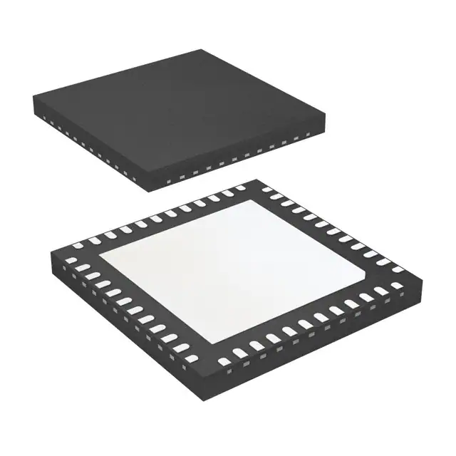
Pin Configuration (48-Pin TQFN)
low" when no display is plugged in
1
VDD
OE#
29
SCL_SINK
30
GND
31
HPD_SINK
32
SDA_SINK
33
DDC_EN
34
GND
VDD
35
28
27
26
25
24
37
IN_D1-
38
23
OUT_D1-
IN_D1+
39
22
OUT_D1+
40
21
VDD
IN_D2-
41
20
OUT_D2-
IN_D2+
42
19
OUT_D2+
GND
43
18
GND
IN_D3-
44
17
OUT_D3-
IN_D3+
45
16
OUT_D3+
VDD
46
15
VDD
IN_D4-
47
14
OUT_D4-
IN_D4+
48
11
13
12
OUT_D4+
VDD
GND
GND
VDD
SR1
GND
6
7
8
9
10
NC
5
SCL_SOURCE
4
SDA_SOURCE
3
HPD_SOURCE
2
NC
1
SR0
GND
VDD
àà 48 TQFN, 7mm × 7mm (ZBE)
36
GND
GND
àà 4kV HBM
àà ±8kV contact ESD protection on the following pins
→→ OUT_Dx±
→→ SDA_SINK, SCL_SINK
→→ HPD_SINK
ÎÎPackaging (Pb-free & Green available):
NC
ÎÎESD protection on all I/O pins
GND
ÎÎTMDS output enable control
NC
ÎÎ3.3V Power supply required
www.pericom.com PS9060A 08/23/11
�PI3VDP411LSR
Dual Mode DisplayPort™ to DVI/HDMI™ Electrical Bridge (Level Shifter)
Block Diagram
OE#
0V
OUTx_D4+
OUTx_D4-
50Ω
50Ω
INx_D4+
Rx
INx_D4-
0V
OUTx_D3+
OUTx_D3-
50Ω
50Ω
INx_D3+
Rx
INx_D3-
0V
OUTx_D2+
OUTx_D2-
50Ω
50Ω
INx_D2+
Rx
INx_D2-
0V
OUTx_D1+
OUTx_D1-
50Ω
50Ω
INx_D1+
Rx
INx_D1SR0
SR1
HPD_SOURCE
HPD
HPD_SINK
100KΩ
DDC_EN (0V to 3.3V)
SDA_Source
SDA_Sink
SCL_Source
SCL_Sink
2
www.pericom.com PS9060A 08/23/11
�PI3VDP411LSR
Dual Mode DisplayPort™ to DVI/HDMI™ Electrical Bridge (Level Shifter)
Pin
Name
I/O Type
Descriptions
1, 5, 12, 18, 24, 27,
31, 36, 37, 43
GND
POWER
GROUND
2, 11, 15, 21, 26, 33,
40, 46
VDD
POWER
POWER, 3.3V ±10%
3
SR0
I
Slew Rate Control. Acceptable connections to SR0 pin are: resistor
to 3.3V or short to GND. (internal 200KΩ pull-LOW)
4
SR1
I
Slew Rate Control. Acceptable connections to SR1 pin are: resistor
to 3.3V or short to GND. (internal 200KΩ pull-LOW)
6, 10, 34, 35
NC
O
No Connect
7
HPD_SOURCE
O
HPD_SOURCE: 0V to 3.3V (nominal) output signal. HPD_Sink
input can be as high as 5V and then HPD_Source will output no
higher than 3.3V.
8
SDA_SOURCE
I/O
3.3V DDC Data I/O. Pulled up by external termination to 3.3V.
Connected to SDA_SINK through voltage limiting integrated
NMOS passgate.
9
SCL_SOURCE
I/O
3.3V DDC Data I/O. Pulled up by external termination to 3.3V.
Connected to SCL_SINK through voltage-limiting integrated
NMOS passgate
13
OUT_D4+
O
HDMI 1.3 compliant TMDS output. OUT_D4+ makes a differential
output signal with OUT_D4-.
14
OUT_D4-
O
HDMI 1.3 compliant TMDS output. OUT_D4- makes a differential
output signal with OUT_D4+
16
OUT_D3+
O
HDMI 1.3 compliant TMDS output. OUT_D3+ makes a differential
output signal with OUT_D3-.
17
OUT_D3-
O
HDMI 1.3 compliant TMDS output. OUT_D3- makes a differential
output signal with OUT_D3+
19
OUT_D2+
O
HDMI 1.3 compliant TMDS output. OUT_D2+ makes a differential
output signal with OUT_D2-.
20
OUT_D2-
O
HDMI 1.3 compliant TMDS output. OUT_D2- makes a differential
output signal with OUT_D2+
22
OUT_D1+
O
HDMI 1.3 compliant TMDS output. OUT_D1+ makes a differential
output signal with OUT_D1-.
23
OUT_D1-
O
HDMI 1.3 compliant TMDS output. OUT_D1- makes a differential
output signal with OUT_D1+
Enable for IN_Dx to OUT_Dx level shifter path.
25
28
OE#
SCL_SINK
I
I/O
OE#
IN_D Termination
OUT_D Outputs
1
> 100KΩ
High-Z
0
50Ω
Active
5V DDC Clock I/O. Pulled up by external termination to 5V.
Connected to SCL_SOURCE through voltage limiting integrated
NMOS passgate.
3
www.pericom.com PS9060A 08/23/11
�PI3VDP411LSR
Dual Mode DisplayPort™ to DVI/HDMI™ Electrical Bridge (Level Shifter)
Pin
Name
I/O Type
Descriptions
29
SDA_SINK
I/O
5V DDC Data I/O. Pulled up by external termination to 5V. Connected to SDA_SOURCE through voltage limiting integrated
NMOS passgate.
I
Low Frequency, 0V to 5V (nominal) input signal. This signal comes
from the TMDS connector. Voltage High indicates “plugged” state;
voltage low indicated “unplugged”. HPD_SINK is pulled down by
an integrated 100K ohm pull-down resistor.
30
HPD_SINK
Enables bias voltage to the DDC passgate level shifter gates. (May
be implemented as a bias voltage connection to the DDC pass gates
themselves.)
32
DDC_EN
I
DDC_EN
Passgate
0V
Disable
3.3V
Enable
38
IN_D1-
I
Low-swing diff input from DP Tx outputs. IN_D1- makes a differential pair with IN_D1+.
39
IN_D1+
I
Low-swing diff input from DP Tx outputs. IN_D1+ makes a differential pair with IN_D1-.
41
IN_D2-
I
Low-swing diff input from DP Tx outputs. IN_D2- makes a differential pair with IN_D2+.
42
IN_D2+
I
Low-swing diff input from DP Tx outputs. IN_D2+ makes a differential pair with IN_D2-.
44
IN_D3-
I
Low-swing diff input from DP Tx outputs. IN_D3- makes a differential pair with IN_D3+.
45
IN_D3+
I
Low-swing diff input from DP Tx outputs. IN_D3+ makes a differential pair with IN_D3-.
47
IN_D4-
I
Low-swing diff input from DP Tx outputs. IN_D4- makes a differential pair with IN_D4+.
48
IN_D4+
I
Low-swing diff input from DP Tx outputs. IN_D4+ makes a differential pair with IN_D4-.
4
www.pericom.com PS9060A 08/23/11
�PI3VDP411LSR
Dual Mode DisplayPort™ to DVI/HDMI™ Electrical Bridge (Level Shifter)
Absolute Maximum Ratings (Over operating free-air temperature range)
Item
Rating
Supply Voltage to Ground Potential
5.5V
All Inputs and Outputs
-0.5V to VDD+0.5V
Ambient Operating Temperature
-40 to +85°C
Storage Temperature
-65 to +150°C
Junction Temperature
150°C
Soldering Temperature
260°C
Stress beyond those listed under “Absolute Maximum Ratings” may cause permanent damage to the device.
Parameter
Min.
Ambient Operating Temperature
Power Supply Voltage (measured in respect to GND)
Max.
Unit
-40
+85
°C
+3.0
+3.6
V
5
Typ.
www.pericom.com PS9060A 08/23/11
�PI3VDP411LSR
Dual Mode DisplayPort™ to DVI/HDMI™ Electrical Bridge (Level Shifter)
Table: Power Supplies and Temperature Range
Symbol
Parameter
Min
Typ
Max
Units
VDD
3.3V Power supply
3.0
3.3
3.6
V
ICC
Max Current
100
mA
ICCQ
Standby Current
2
mA
TCASE
Case temperature range
for operation with spec.
85
Celsius (°)
Max
Units
Comments
ps
Tbit is determined by the display
mode. Nominal bit rate ranges from
250Mbps to 2.5Gbps per lane. Nominal Tbit at 2.5 Gbps = 400 ps. 360ps =
400ps-10%
V
See note 1 below
Tbit
The level shifter may add a maximum
of 0.02UI jitter (400 * 0.02) = 8ps
100
mV
See note 2 below
60
Ω
Required IN_D+ as well as IN_D- DC
impedance (50 ±20% tolerance).
2.0
V
Intended to limit power-up stress on
chipset's PCIE output buffers.
kΩ
Differential inputs must be in a high
impedance state when OE# is HIGH.
-40
Comments
OE# = HIGH
Table: Differential Input Characteristics for IN_Dx signals
Symbol
Parameter
Min
Tbit
Unit Interval
360
VRX_DIFF
Input Differential Voltage level
0.175
TRX_EYE
Minimum Eye Width at
IN_D input pair
0.8
VCM-ACp-p
AC Peak Common
Mode Input Voltage
ZRX_DC
40
ZRX-Bias
0
ZRX_HIGH-Z
100
Typ
1.200
50
1. VRX-DIFF = 2x|VRX-D- -VRX-D-| Applies to IN_Dx signals
2. VCM-AC-p-p = |VRX-D - - VRX-D -|/2 - VRX-CM-DC
VRX-CM-DC = DC(avg) of |VRX-D+ + VRX-D -|/2
VCM-AC-p-p includes all frequencies above 30 kHz.
TMDS Outputs
The level shifter's TMDS outputs are required to meet HDMI 1.3 specifications.
The HDMI 1.3 Specification is assumed to be the correct reference in instances where this document conflicts with the HDMI 1.3
specification.
6
www.pericom.com PS9060A 08/23/11
�PI3VDP411LSR
Dual Mode DisplayPort™ to DVI/HDMI™ Electrical Bridge (Level Shifter)
Truth Table (Slew Rate control function)
SR1
SR0
Rise/Fall Time (Typ)
1
1
140ps
1
0
130ps
0
1
120ps
0
0
110ps
Test Setup Condition
VDD = 3.3V, Ambient temperture 25°C
Rise/Fall time is from 20% to 80% on Rising/Falling edge
Date rate: 620 Mbps
Input: 1V differential peak-to-peak clock pattern
Equalization : 3dB
Table 1: OE Pin Description
OE#
Device State
Comments
Asserted (low voltage)
Differential input buffers and output buffers
enabled. Input impedance = 50Ω
Normal functioning state for IN_D to OUT_D
level shifting function.
Low-power state.
Unasserted (high voltage)
àà Differential input buffers and termination Intended for lowest power condition when:
àà No display is plugged in or
are disabled.
àà The level shifted data path is disabled
àà Differential inputs are in a high
HPD_SINK input and HPD_SOURCE
impedance state.
output are not affected by OE# SCL_
àà OUT_D level-shifting outputs are
SOURCE, SCL_SINK, SDA_SOURCE
disabled.
and SDA_SINK signals and functions
àà OUT_D level-shifting outputs are in high
are not affected by OE#
impedance state.
àà Internal bias currents are turned off.
7
www.pericom.com PS9060A 08/23/11
�PI3VDP411LSR
Dual Mode DisplayPort™ to DVI/HDMI™ Electrical Bridge (Level Shifter)
Table 2: Differential Output Characteristics for TMDS_OUT signals
Symbol
Parameter
Min
Typ
Max
Units
Comments
VH
Single-ended high level
output voltage
VDD -10mV
VDD
VDD+10mV
V
VDD is the DC termination voltage in the HDMI or DVI Sink.
VDD is nominally 3.3V
VL
Single-ended low level
output voltage
VDD -600mV VDD -500mV VDD -400mV V
VSWING
Single ended output swing
425
voltage
IOFF
Single-ended current in
high-Z state
500
The open-drain output pulls
down from VDD.
600
mV
Swing down from TMDS termination voltage (3.3V ±10%)
50
µA
Measured with TMDS outputs
pulled up to VDD Max _(3.6V)
through 50Ω resistors.
TSKEW-INTRA
Intra-pair differential
skew
30
ps
This differential skew budget is
in addition to the skew presented between D+ and D- paired
input pins. HDMI revision 1.3
source allowable intrapair skew
is 0.15 Tbit.
TSKEW-INTER
Inter-pair lane-to-lane
output skew
100
ps
This lane-to-lane skew budget
is in addition to skew between
differential input pairs
TJIT
Jitter added to TMDS
signals
ps
Jitter budget for TMDS signals
as they pass through the level
shifter. 25ps = 0.056 Tbit at 2.25
Gb/s
25
TMDS output oscillation elimination
The inputs do not incorporate a squelch circuit. Therefore, we recommend the input to be externally biased to prevent output oscillation. Pericom recommends to add a 1.5Kohm pull-up to the CLK- input.
VBIAS
3.3V
1.5Kohm
RINT
RINT
DMDP
Receiver
TMDS
Driver
SS
RT
AVDD
SS
RT
TMDS Input Fail-Safe Recommendation
8
www.pericom.com PS9060A 08/23/11
�PI3VDP411LSR
Dual Mode DisplayPort™ to DVI/HDMI™ Electrical Bridge (Level Shifter)
Table 3: HPD Characteristics
Symbol
Parameter
Min
Typ
Max
Units
Comments
VIH-HPD
Input High Level
2.0
5.0
5.3
V
Low-speed input changes state on cable plug/
unplug
VIL-HPD
HPD_sink Input Low
Level
0
0.8
V
IIN-HPD
HPD_sink Input Leakage
Current
70
µA
VOH-HPD
HPD_source Output
High-Level
VDD
V
VOL-HPD
HPD_source Output Low0
Level
0.4
V
IOL = 4mA(MIN) / 8mA(MAX)
THPD
HPD_sink to HPD_source
propagation delay
200
ns
Time from HPD_sink changing state to
HPD_source changing state. Includes HPD_
source rise/fall time
TRF-HPDB
HPD_source rise/ fall time 1
20
ns
Time required to transition from VOH- HPDB
to VOL-HPDB or from VOL-HPDB to VOH-HPDB
Max
Units
Comments
TMDS enable input changes state on cable
plug/unplug
2.5
Measured with HPD_sink at VIH-HPD max
and VIL-HPD min
VDD = 3.3V ±10%
IOH = -4mA(MIN) / -8mA(MAX)
Table 4: OE# Input, DDC_EN
Symbol
Parameter
Min
Typ
VIH
Input High Level
2.0
VDD
V
VIL
Input Low Level
0
0.8
V
IIN
Input Leakage Current
10
µA
Measured with input at VIH-EN max and
VIL-EN min
Max
Units
Comments
Ω
Guarantees HPD_sink is LOW when no
display is plugged in.
Table 5: Termination Resistor
Symbol
Parameter
Min
R HPD
HPD_sink input pulldown resistor.
100K
Typ
9
www.pericom.com PS9060A 08/23/11
�PI3VDP411LSR
Dual Mode DisplayPort™ to DVI/HDMI™ Electrical Bridge (Level Shifter)
UNIT: mm
1
DATE: 02/11/09
Notes:
1. All dimensions are in millimeters, angles are in degrees.
2. Coplanarity applies to the exposed thermal pad as well as the terminals.
3. Refer JEDEC MO-220
4. Recommended land pattern is for reference only.
5. Thermal pad soldering area
DESCRIPTION: 48-Pin, Thin Fine Pitch Quad Flat No-Lead (TQFN)
PACKAGE CODE: ZB48
DOCUMENT CONTROL #: PD-2080
REVISION: A
09-0091
Note:
• For latest package info, please check: http://www.pericom.com/products/packaging/mechanicals.php
Ordering Information
Ordering Code
Package Code
Package Type
PI3VDP411LSRZBE
ZB
Pb-free & Green, 48-pin TQFN
1. Thermal characteristics can be found on the company web site at www.pericom.com/packaging/
2. E = Pb-free and Green
3. Adding an X suffix = Tape/Reel
Pericom Semiconductor Corporation • 1-800-435-2336
10
DisplayPort is a trademark of VESA www.vesa.org
HDMI, High-Definition Multimedia Interface, and Deep Color are trademarks of HDMI Licensing, LLC in the United States and other countries.
www.pericom.com PS9060A 08/23/11
�
很抱歉,暂时无法提供与“PI3VDP411LSRZBE”相匹配的价格&库存,您可以联系我们找货
免费人工找货