PI3VeDP212
2-lane DisplayPort™ Switch/Mux for
DP Driven Panels with Triple Control Pins
Features
Description
• 2 Differential Channel, 2:1 mux/demux that will support
2.7Gbps or 1.62Gbps DP signals
• 1-differential channel is used for AUX signaling
• Insertion Loss for high speed channels @ 2.7 Gbps: -1.5dB
• Hot Insertion Cable
• -3dB Bandwidth for high speed channels of 3.25 Ghz
• Low Bit-to-Bit Skew , 7ps max (between '+' and '-' bits)
• Low Crosstalk for high speed channels: -33dB@2.7 Gbps
• Low Off Isolation for high speed channels: -26dB@2.7 Gbps
• VDD Operating Range: 3.3V +/-10%
• ESD Tolerance: 8kV HBM on all data I/O pins per JESD22
Specification
• Low channel-to-channel skew, 35ps max
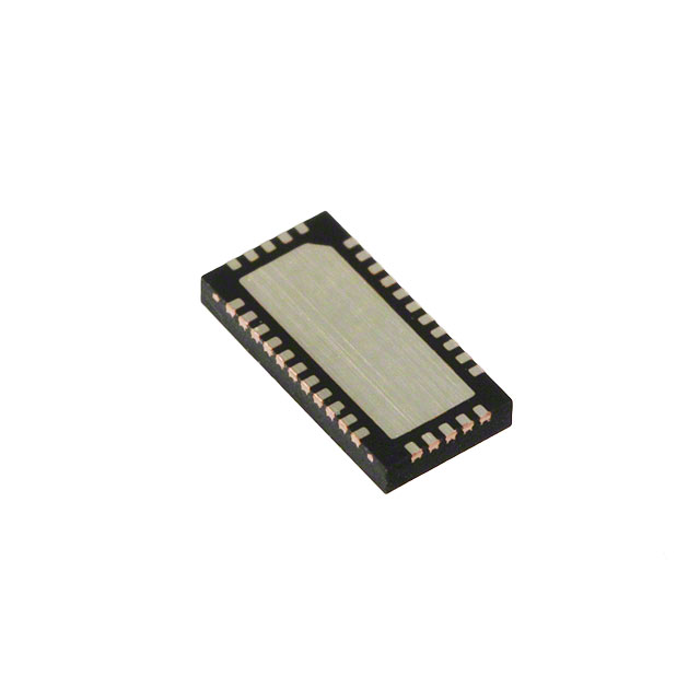
• Packaging (Pb-free & Green):
- 32 TQFN (ZLE)
Pericom Semiconductor’s PI3VeDP212 switch is targeted for
next generation digital video signals. This device can be used to
connect two DisplayPortTM sources to a single panel.
The newly released DisplayPort spec requires a data rate of
2.7 Gbps with AC coupled I/Os. Pericom's solution has been
specifically designed around this standard and will support such
signals.
Block Diagram
Pin Description
Application
AUX_SEL
D0+A
D0-A
VDD
GND
Routing of DisplayPortTM signals with low signal attenuation between notebook DP connector and docking station DP connector.
D0+A
D0-A
D1+A
D1-A
D0+
D0 D1+
D1 -
D0+B
D0-B
D1+B
D1-B
AUX+
AUXHPD
D0+
D0VDD
D1+
D1AUX+
AUXHPD
VDD
SEL
HPD_SEL
AUX+�A
AUX-�A
HPD�A
AUX+�B
AUX-�B
HPD�B
HPD_SEL
SEL
2
26
3
25
4
24
5
23
6
22
7
21
8
20
9
19
10
18
11
17
12 13 14 15 16
D1+A
D1-A
D0+B
D0-B
D1+B
D1-B
GND
VDD
AUX+A
AUX-A
HPD_A
VDD
HPD_B
AUX-B
AUX+B
VDD
AUX_SEL
Logic
Control
32 31 30 29 28
1
27
11-0082
1
PS9057A
08/23/11
�PI3VeDP212
2-lane DisplayPort™ Switch/Mux for
DP Driven Panels with Triple Control Pins
Truth Table (SEL control)
Function
SEL /HPD_SEL/AUX_SEL
Port A is active
L
Port B is active
H
Notes: SEL only controls main DP lanes
HPD_SEL only controls HPD signaling
AUX_SEL only controls AUX signaling
11-0082
2
PS9057A
08/23/11
�PI3VeDP212
2-lane DisplayPort™ Switch/Mux for
DP Driven Panels with Triple Control Pins
Maximum Ratings
(Above which useful life may be impaired. For user guidelines, not tested.)
Storage Temperature .....................................................–65°C to +150°C
Supply Voltage to Ground Potential ................................–0.5V to +3.6V
DC Input Voltage ............................................................... –0.5V to 3.6V
DC Output Current ....................................................................... 120mA
Power Dissipation ............................................................................ 0.5W
Note: Stresses greater than those listed under MAXIMUM
RATINGS may cause permanent damage to the device. This
is a stress rating only and functional operation of the device
at these or any other conditions above those indicated in the
operational sections of this specification is not implied. Exposure to absolute maximum rating conditions for extended
periods may affect reliability.
DC Electrical Characteristics for Switching over Operating Range (TA = –40°C to +85°C, VDD = 3.3V +/-10%)
Parameter
VIH
VIL
Test Conditions(1)
Description
Min
Typ(2)
Max
Units
0.65
V
Input HIGH Voltage
Guaranteed HIGH level
1.5
Input LOW Voltage
Guaranteed LOW level
–0.5
VIK
IIH
Clamp Diode Voltage
VDD = Max., IIN = –18mA
Input HIGH Current
VDD = Max., VIN = VDD
±5
IIL
Input LOW Current
VDD = Max., VIN = GND
±5
IOFF
I/O leakage when part is off
VDD = 0V, Vinput = 0V to 3.6V
50
Power Supply Characteristics (TA = 0°C to +70°C)
Parameters
ICC
Test Conditions(1)
Description
Quiescent Power Supply Current
–0.7
Min.
–1.2
Typ.(2)
µA
Max.
Units
70
µA
VDD = Max., VIN = GND or VDD
Dynamic Electrical Characteristics Over the Operating Range (TA= -40º to +85ºC, VDD = 3.3V +/-10%,
GND=0V)
Parameter
Description
XTALK
Crosstalk on High
Speed Channels
OIRR
OFF Isolation on
High Speed Channels
ILOSS
Differential
Insertion Loss on
High Speed Channels
BW
Bandwidth -3dB
Typ.(2)
Test Conditions
See Fig. 1 for Measurement Setup
See Fig. 2 for Measurement Setup,
@2.7Gbps
See Fig. 3 for Differential Insertion Loss
f= 1.35 GHz
-33dB
f = 100 MHz
-48dB
f= 1.35 GHz
-33dB
f = 100 MHz
-56dB
Units
dB
-1.5
dB
3.25
GHz
Notes:
1. For Max. or Min. conditions, use appropriate value specified under Electrical Characteristics for the applicable device type.
2. Typical values are at VDD = 3.3V, Ta = 25°C ambient and maximum loading.
11-0082
3
PS9057A
08/23/11
�PI3VeDP212
2-lane DisplayPort™ Switch/Mux for
DP Driven Panels with Triple Control Pins
BALANCED
PORT1
BALANCED
PORT2
+
+
50
–
–
50
+
+
50
–
–
50
DUT
Fig 1. Crosstalk Setup
BALANCED
PORT1
+
+
50
–
–
50
+
BALANCED
PORT2
–
DUT
Fig 2. Off-isolation setup
BALANCED
PORT1
+
+
–
–
BALANCED
PORT2
DUT
Fig 3. Differential Insertion Loss
11-0082
4
PS9057A
08/23/11
�PI3VeDP212
2-lane DisplayPort™ Switch/Mux for
DP Driven Panels with Triple Control Pins
Fig 4. Crosstalk
Fig 5. Off Isolation
11-0082
5
PS9057A
08/23/11
�PI3VeDP212
2-lane DisplayPort™ Switch/Mux for
DP Driven Panels with Triple Control Pins
Fig 5. Insertion Loss
Fig 6. Insertion Loss
Fig 7. Ron Curve for High Speed Signal Path Only (Dx+/-)
11-0082
6
PS9057A
08/23/11
�PI3VeDP212
2-lane DisplayPort™ Switch/Mux for
DP Driven Panels with Triple Control Pins
Switching Characteristics (TA= -40º to +85ºC, VDD = 3.3V±10%)
Parameter
Description
Min.
Max.
Units
tPZH, tPZL
Line Enable Time
0.5
15.0
tPHZ, tPLZ
Line Disable Time
0.5
15.0
tb-b
Bit-to-bit skew within the same differential pair
7
ps
tch-ch
Channel-to-channel skew
50
ps
ns
Test Circuit for Electrical Characteristics(1-5)
6.0V
VDD
200-ohm
Pulse
Generator
VIN
VOUT
D.U.T
4pF
CL
RT
200-ohm
Notes:
1. CL = Load capacitance: includes jig and probe capacitance.
2. RT = Termination resistance: should be equal to ZOUT of the Pulse Generator
3. Output 1 is for an output with internal conditions such that the output is low except when disabled by the output control.
output 2 is for an output with internal conditions such that the output is high except when disabled by the output control.
4. All input impulses are supplied by generators having the following characteristics: PRR ≤ MHz, ZO = 50Ω, tR ≤ 2.5ns, tF ≤ 2.5ns.
5. The outputs are measured one at a time with one transition per measurement.
Switching Waveforms
SEL
VDD/2
VDD/2
VDD
0V
Output 1
tPZL
tPLZ
VDD/2
VOH
VOL + 0.3V
tPHZ
tPZH
VOH – 0.3V
VDD/2
VOL
VOH
VOL
Output 2
Voltage Waveforms Enable and Disable Times
Switch Positions
Test
Switch
tPLZ, tPZL (output on B-side)
6.0V
tPHZ, tPZH (output on B-side)
GND
Prop Delay
Open
11-0082
7
PS9057A
08/23/11
�PI3VeDP212
2-lane DisplayPort™ Switch/Mux for
DP Driven Panels with Triple Control Pins
Test Circuit for Dynamic Electrical Characteristics
Agilent N5230A 300kHz-20GHz PNA-L Network Analyzer
R1
S1
T1
PI3VDP130
HP11667A
Packaging Mechanical: 32-Contact TQFN (ZL)
1
DATE: 10/09/09
DESCRIPTION: 32-contact, Thin Fine Pitch Quad Flat No-Lead (TQFN)
PACKAGE CODE: ZL (ZL32)
REVISION: A
DOCUMENT CONTROL #: PD-2044
09-0125 Information
Ordering
Ordering Code
PI3VeDP212ZLE
Package Code
Package Description
ZL
Pb-free and Green 32-Contact TQFN
Notes:
• Thermal characteristics can be found on the company web site at www.pericom.com/packaging/
• "E" denotes Pb-free and Green
• Adding an "X" at the end of the ordering code denotes tape and reel packaging
11-0082
DisplayPort is a trademark of VESA www.vesa.org
8
PS9057A
08/23/11
�
很抱歉,暂时无法提供与“PI3VEDP212ZLE”相匹配的价格&库存,您可以联系我们找货
免费人工找货