A product Line of
Diodes Incorporated
PI3WVR31310A
DP/HDMI 1:3 De-mux/Mux Switches
Features
Description
ÎÎDP 1:3 De-Mux or 3:1 Mux switch with 4 high speed
The PI3WVR31310A is a 3:1 Mux or 1:3 Demux high speed passive switch supporting DP 1.2, HDMI 1.4, HDMI 2.0. At DEMUX
mode, all three output ports support auto port priority selection by detecting HPD1/2/3 input or manual selection. At MUX
mode, HPD1/2/3 will change from input to output, there is no
auto port priority selection.
differential, AUX/DDC, HPD and CAB_DET channels
ÎÎPin selection for 1:3 DEMUX or 3:1 MUX
ÎÎHDMI 3:1 Mux switch with 4 high speed differential, DDC
and HPD channels
ÎÎHDMI-mode only supports HDMI-sink application, not
support HDMI-source application.
ÎÎPin selection for DP mode or HDMI mode
Application
ÎÎAll ports support up to DP1.2 at 5.4Gb/s or HDMI 2.0 at
ÎÎNotebook, Monitor, Switch box or TV sink application
6Gb/s
ÎÎSupports manual switching or HPD auto priority selection
in 1:3 DEMUX, in DP mode
ÎÎLow current consumption
ÎÎ3.3V power supply
ÎÎESD protection on all I/O pins for 2kV HBM
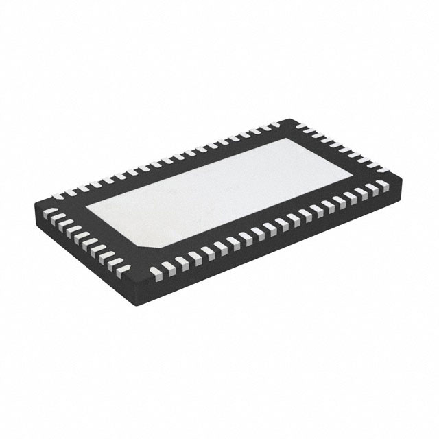
ÎÎPackage:
60 pin TQFN (5x9mm)
Block Diagram
CAB_SRC HPD_SRC
MUX
DEMUX
120KΩ[1]
Control
Block
[1]
HPD1
[1]
HPD2
[1]
HPD3
120KΩ
120KΩ
120KΩ
CAB_1
CAB_2
CAB_3
AUX1P/SCL1
AUX1N/SDA1
AUX2P/SCL2
AUX2N/SDA2
AUX3P/SCL3
AUX3N/SDA3
AUXP
AUXN
SDA
SCL
D[0:3]P1
D[0:3]N1
D[0:3]P2
D[0:3]N2
D[0:3]P
D[0:3]N
D[0:3]P3
D[0:3]N3
Port select
OEB
PRI_SEL
SEL1
SEL0
DP_HDMI
DEMUX_MUX
All trademarks are property of their respective owners.
Control & Status
Register
17-0002
1
www.diodes.com 01/09/17
�A product Line of
Diodes Incorporated
PI3WVR31310A
D0P1
D0N1
D1P1
D1N1
D2P1
D2N1
D3P1
D3N1
PRI_SEL
OEB
Pin Configuration: TQFN-60
60 59 58 57 56 55 54 53 52 51
VDD
D0P
D0N
D1P
D1N
D2P
D2N
D3P
D3N
SEL1
SEL0
HPD_SRC
CAB_SRC
CAB_3
HPD3
DEMUX_MUX
AUXP
AUXN
SCL
SDA
1
2
3
4
5
6
7
8
9
10
11
12
13
14
15
16
17
18
19
20
GND
TQFN-60
5x9 mm
50
49
48
47
46
45
44
43
42
41
40
39
38
37
36
35
34
33
32
31
VDD
D0P2
D0N2
D1P2
D1N2
D2P2
D2N2
D3P2
D3N2
D0P3
D0N3
D1P3
D1N3
D2P3
D2N3
D3P3
D3N3
VDD
AUX1P/SCL1
AUX1N/SDA1
VDD
DP_HDMI
AUX3N/SDA3
AUX3P/SCL3
CAB_2
HPD2
AUX2N/SDA2
AUX2P/SCL2
CAB_1
HPD1
21 22 23 24 25 26 27 28 29 30
Note: 1. The 120kΩ pull down resistor is not always on.
All trademarks are property of their respective owners.
17-0002
2
www.diodes.com 01/09/17
�A product Line of
Diodes Incorporated
PI3WVR31310A
Pin Description
pin#
pin Name
2,
D0P,
4,
D1P,
6,
D2P,
8,
D3P,
3,
D0N,
5,
D1N,
7,
D2N,
9
D3N
60,
D0P1,
58,
D1P1,
56,
D2P1,
54,
D3P1,
59,
D0N1,
57,
D1N1,
55,
D2N1,
53
D3N1
49,
D0P2,
47,
D1P2,
45,
D2P2,
43,
D3P2,
48,
D0N2,
46,
D1N2,
44,
D2N2,
42
D3N2
41,
D0P3,
39,
D1P3,
37,
D2P3,
35,
D3P3,
40,
D0N3,
38,
D1N3,
36,
D2N3,
34
D3N3
All trademarks are property of their respective owners.
Signal Type
17-0002
Description
IO
4 differential pair I/O (DP or HDMI)
IO
4 differential pair I/O (DP or HDMI) for port 1
IO
4 differential pair I/O (DP or HDMI) for port 2
IO
4 differential pair I/O (DP or HDMI) for port 3
3
www.diodes.com 01/09/17
�A product Line of
Diodes Incorporated
PI3WVR31310A
pin#
pin Name
31,
AUX1N/SDA1,
27,
AUX2N/SDA2,
23,
AUX3N/SDA3,
32,
AUX1P/SCL1,
28,
AUX2P/SCL2,
24
AUX3P/SCL3
18,
AUXN,
17
AUXP
20,
SDA,
19
SCL
30,
HPD1,
26,
HPD2,
15,
HPD3,
12
HPD_SRC
29,
CAB_1,
25,
CAB_2,
14,
CAB_3,
13
CAB_SRC
51
OEB
Signal Type
Description
IO
AUX (DP) or DDC (HDMI) input from three ports
IO
AUX output
IO
DDC output
IO
IO
When DEMUX_MUX = low (1:3 DEMUX mode), HPD1_2_3
are inputs, HPD_SRC is output;
When DEMUX_MUX = high (3:1 MUX mode), HPD1_2_3 are
outputs, HPD_SRC is input
CAB_1, CAB_2, CAB_3, CAB_SRC
I
OEB=0, device active; OEB=1, device shut down
52
PRI_SEL
I
PRI_SEL is for priority selection as in priority-selection-table,
but only for 1:3 DEMUX mode. PRI_SEL has internal 100K
divider between VDD and GND for middle-state with VDD/2.
16
DEMUX_MUX
I
DEMUX_MUX is for HPD direction selection, see truth table
22
DP_HDMI
I
DP port or HDMI port, see truth table
11
SEL0
I
Port selection pins, see truth table
10
SEL1
I
Port selection pins, see truth table
1, 21, 33, 50
VDD
Power
Center Pad
GND
Ground
All trademarks are property of their respective owners.
17-0002
3.3V VDD
Bottom GND EPAD
4
www.diodes.com 01/09/17
�A product Line of
Diodes Incorporated
PI3WVR31310A
Pin mapping for dual mode DP source DEMUX to DP output
DP mode
HDMI/DVI mode
WVR31310A WVR31310A
input pins
port1 output
WVR31310A
port2 output
WVR31310A
port3 output
DP mode
ML_lan0(P)
TX2+
D0P
D0P1
D0P2
D0P3
ML_lan0(P)
ML_lan0(N)
TX2-
D0N
D0N1
D0N2
D0N3
ML_lan0(N)
ML_lan1(P)
TX1+
D1P
D1P1
D1P2
D1P3
ML_lan1(P)
ML_lan1(N)
TX1-
D1N
D1N1
D1N2
D1N3
ML_lan1(N)
ML_lan2(P)
TX0+
D2P
D2P1
D2P2
D2P3
ML_lan2(P)
ML_lan2(N)
TX0-
D2N
D2N1
D2N2
D2N3
ML_lan2(N)
ML_lan3(P)
TXC+
D3P
D3P1
D3P2
D3P3
ML_lan3(P)
ML_lan3(N)
TXC-
D3N
D3N1
D3N2
D3N3
ML_lan3(N)
Function Description
Default input format is DP. DP_HDMI can select between DP or HDMI input.
In Demux mode, there are 120K pull down in HPD1/HPD2/HPD3 pins. In Mux mode, there is 120K pull down in HPD_SRC pin.
Output port can be selected by manual or automatically in DEMUX mode.
Automatic port selection is done by detection of HPD presence from the output ports. If multiple HPD are detected, port selection
depends on a priority scheme defined by PRI_SEL pin. There can be 3 priority schemes. When PRI_SEL=low, the port priority order
is port1/port2/port3; when PRI_SEL=high, the port priority order is port2/port3/port1; when PRI_SEL=M (open), the port priority
order is port3/port1/port2.
When port 1 or port 2 or port 3 is selected in DP application, and CAB=LOW, AUX/DDC input pins are now AUX channel. AUXP
will have 100Kohm resistor to GND while AUXN will have 100Kohm resistor to VDD in external port side. Max. AUX data rate
can be 720Mb/s. DDC switch inside is off.
When port 1 or port 2 or port 3 is active in dual mode DP or HDMI application, and CAB=HIGH, AUX/DDC input pins are now
DDC channel. AUX switch inside is off, DDC switch is on. The DDC switch can support 5V input, and output Vpass is less than
3.3V limit.
HPD is CMOS buffer, and support 5v inputs. When used as DEMUX, There’re 120kΩ pull-down resistors inside connected to
HPD1, HPD2, HPD3 as input, and when used as MUX, 120k resistor connected to HPD_SRC as input.
All trademarks are property of their respective owners.
17-0002
5
www.diodes.com 01/09/17
�A product Line of
Diodes Incorporated
PI3WVR31310A
Truth Table
DEMUX_MUX
DP_HDMI
DEMUX_MUX
HPD_SRC
HPD1/2/3
DP_HDMI
Mode
0 (DEMUX)
output
input
0
DP Mode
1 (MUX)
input
output
1
HDMI Mode
SLE1/SEL0 in 1:3 DP modes
SEL1
SEL0
PRI_SEL
(priority selection)
0
0
NC
HPD1/CAB_1
Port 1
0
1
NC
HPD2/CAB_2
Port 2
1
0
NC
HPD3/CAB_3
Port 3
1
1
Auto-selection
See priority table
See priority table
HPD
D[0:3]P, D[0:3]N, AUX/DDC
HPD/CAB_DET
D[0:3]P, D[0:3]N, AUX/DDC
SLE1/SEL0 in 3:1 HDMI mode and DP mode
SEL1
SEL0
PRI_SEL
(priority selection)
0
0
NC
HPD=HPD1, HPD2/3=0
Port 1
0
1
NC
HPD=HPD2, HPD1/3=0
Port 2
1
0
NC
HPD=HPD3, HPD1/2=0
Port 3
1
1
NC
NC
NC
AUX and DDC
PORT
When Port1
Selected
When Port2
Selected
When Port3
Selected
DP_HDMI
CAB_1
CAB_2
CAB_3
AUXP
AUXN
SCL
SDA
0
0
x
x
AUX1P
AUX1N
Hi-Z
Hi-Z
0
1
x
x
Hi-Z
Hi-Z
SCL1
SDA1
1
1
x
x
Hi-Z
Hi-Z
SCL1
SDA1
0
x
0
x
AUX2P
AUX2N
Hi-Z
Hi-Z
0
x
1
x
Hi-Z
Hi-Z
SCL2
SDA2
1
x
1
x
Hi-Z
Hi-Z
SCL2
SDA2
0
x
x
0
AUX3P
AUX3N
Hi-Z
Hi-Z
0
x
x
1
Hi-Z
Hi-Z
SCL3
SDA3
1
x
x
1
Hi-Z
Hi-Z
SCL3
SDA3
All trademarks are property of their respective owners.
17-0002
6
www.diodes.com 01/09/17
�A product Line of
Diodes Incorporated
PI3WVR31310A
Priority Selection Table
PRI_SEL
(Priority order)
HPD1
HPD2
HPD3
HPD_SRC
CAB_SRC
AUXP/AUXN
SDA/SCL
0
0
0
0
0
Hi-Z
Hi-Z
Hi-Z
0
1
x
x
HPD1
CAB1
AUX1P/AUX1N
SDA1/SCL1
0
0
1
x
HPD2
CAB2
AUX2P/AUX2N
SDA2/SCL2
0
0
0
1
HPD3
CAB3
AUX3P/AUX3N
SDA3/SCL3
M
0
0
0
0
Hi-Z
Hi-Z
Hi-Z
M
1
x
0
HPD1
CAB1
AUX1P/AUX1N
SDA1/SCL1
M
0
1
0
HPD2
CAB2
AUX2P/AUX2N
SDA2/SCL2
M
x
x
1
HPD3
CAB3
AUX3P/AUX3N
SDA3/SCL3
1
0
0
0
0
Hi-Z
Hi-Z
Hi-Z
1
1
0
0
HPD1
CAB1
AUX1P/AUX1N
SDA1/SCL1
1
x
1
x
HPD2
CAB2
AUX2P/AUX2N
SDA2/SCL2
1
x
0
1
HPD3
CAB3
AUX3P/AUX3N
SDA3/SCL3
Note: M= VDD/2 or open (with internal VDD/2)
PRI_SEL
(Priority order) HPD1
HPD2
HPD3
D0P
D1P
D2P
D3P
D0N
D1N
D2N
D3N
0
0
0
0
Hi-Z
Hi-Z
Hi-Z
Hi-Z
Hi-Z
Hi-Z
Hi-Z
Hi-Z
0
1
x
x
D0P1
D1P1
D2P1
D3P1
D0N1
D1N1
D2N1
D3N1
0
0
1
x
D0P2
D1P2
D2P2
D3P2
D0N2
D1N2
D2N2
D3N2
0
0
0
1
D0P3
D1P3
D2P3
D3P3
D0N3
D1N3
D2N3
D3P3
M
0
0
0
Hi-Z
Hi-Z
Hi-Z
Hi-Z
Hi-Z
Hi-Z
Hi-Z
Hi-Z
M
1
x
0
D0P1
D1P1
D2P1
D3P1
D0N1
D1N1
D2N1
D3N1
M
0
1
0
D0P2
D1P2
D2P2
D3P2
D0N2
D1N2
D2N2
D3N2
M
x
x
1
D0P3
D1P3
D2P3
D3P3
D0N3
D1N3
D2N3
D3P3
1
0
0
0
Hi-Z
Hi-Z
Hi-Z
Hi-Z
Hi-Z
Hi-Z
Hi-Z
Hi-Z
1
1
0
0
D0P1
D1P1
D2P1
D3P1
D0N1
D1N1
D2N1
D3N1
1
x
1
x
D0P2
D1P2
D2P2
D3P2
D0N2
D1N2
D2N2
D3N2
1
x
0
1
D0P3
D1P3
D2P3
D3P3
D0N3
D1N3
D2N3
D3P3
Note: M= VDD/2 or open (with internal VDD/2)
Note: For priority selection control, when PRI_SEL = 0, the order is port1/port2/port3; when PRI_SEL = 1, the order is port2/port3/port1; when PRI_SEL = M, the
order is port3/port1/port2.
All trademarks are property of their respective owners.
17-0002
7
www.diodes.com 01/09/17
�A product Line of
Diodes Incorporated
PI3WVR31310A
Maximum Ratings
(Above which useful life may be impaired. For user guidelines not tested.)
Storage Temperature ........................................................... –65°C to +150°C
Supply Voltage to Ground Potential ....................................–0.5V to +4.6V
High Speed Channel Input Voltage (DP Mode)........................–0.5V to 2V
High Speed Channel Input Voltage (HDMI Mode)................2.4V to 3.6V
DDC and HPD channels Input Voltage ....................................–0.5V to 6V
DC Output Current ................................................................................ 40mA
Power Dissipation .................................................................................... 0.2W
Note: Stresses greater than those listed under MAXIMUM
RATINGS may cause permanent damage to the device.
This is a stress rating only and functional operation of the
device at these or any other conditions above those indicated in the operational sections of this specification is not
implied. Exposure to absolute maximum rating conditions
for extended periods may affect reliability.
Electrical Characteristics
Recommended Operation Conditions
VDD = 3.3V ±10%, Min and Max apply for TA between -40oC to 85oC Typical values are referenced to TA = 25oC
Parameter
Description
VDD
Operating Voltage
IDD
VDD supply current
Test Conditions
Min.
Typ.
Max.
Unit
3.0
3.3
3.6
V
VDD=3.3V
Supply current when OEB disable VDD=3.6V, OEB=high
Istd
DP_HDMI=1
HDMI Mode
Supply current when OEB disable VDD=3.6V, OEB=high
DP_HDMI=0
DP Mode
1
mA
0.7
mA
10
uA
DC Electrical Characteristics for Switching over Operating Range
Parameter
Description
Test Conditions
Min.
Typ.
Max.
Unit
IIH
High level digital input current
VIH =VDD
-10
40
μA
IIL
Low level digital input current
VIL = GND
-10
10
μA
VIH
High level digital input voltage
2.0
VIL
Low level digital input voltage
0
0.8
V
OEB, SEL1, SEL0
V
DEMUX_MUX
IIH
High level digital input current
VIH =VDD
-10
40
μA
IIL
Low level digital input current
VIL = GND
-10
10
μA
VIH
High level digital input voltage
2.7
VIL
Low level digital input voltage
0
V
0.8
V
DP_HDMI
Rpd
Inter Pull-down resistor on
DP_HDMI
VIH
High level digital input voltage
0.7Vdd
VIL
Low level digital input voltage
0
All trademarks are property of their respective owners.
17-0002
100
8
kΩ
V
0.3Vdd
V
www.diodes.com 01/09/17
�A product Line of
Diodes Incorporated
PI3WVR31310A
Parameter
Description
Test Conditions
Min.
Typ.
Max.
Unit
HPD_SRC (when HPD_SRC is output, HPD 1, 2, 3 are inputs)
VIH
High level digital input voltage
VDD=3.3V
2.0
VIL
Low level digital input voltage
VDD=3.3V
0
VOL_HPD_SRC
Buffer Output Low Voltage
IOL = 4 mA
VOH_HPD_SRC
Buffer Output Low Voltage
IOH = 4 mA
V
0.8
V
0.4
V
2.4
V
2.0
V
HPD_Sink (when HPD_SRC is input, HPD 1, 2, 3 are as sink outputs)
VIH
High level digital input voltage
VIL
Low level digital input voltage
VOL_HPD_Sink
Buffer Output Low Voltage
IOL = 4 mA
VOH_HPD_Sink
Buffer Output Low Voltage
IOH = 4 mA
2.4
ILK
Input leakage current
Switch is off, Vin=5.5V
-50
CIO
Input/Output capacitance when
passive switch on
RON
Passive Switch resistance
IO = 3mA, VO = 0.4V
Vpass
Switch Output voltage
VI=3.3V, II=100uA
CI(source)
Source side CAB capacitance
CI(sink)
Sink side CAB capacitance when
VDD=3.3V
0
0.8
V
0.4
V
V
CAB
50
10
3.0
VI peak-peak = 1V, 100 KHz
uA
pF
25
50
Ω
3.5
4.0
V
3.5
pF
6.5
pF
SDA/SCL,SDA1/SCL1, SDA2/SCL2 , SDA3/SCL3 (passive switch)
ILK
Input leakage current
DDC switch is off, Vin=5.5V
CIO
Input/Output capacitance when
passive switch on
VI peak-peak = 1V, 100 KHz
10
RON
Passive Switch resistance
IO = 3mA, VO = 0.4V
25
50
Ω
Vpass
Switch Output voltage
2.0
2.5
V
CI(source)
Source side DDC capacitance (
passive switch off. )
CI(sink)
Sink side DDC capacitance ( pasVI peak-peak = 1V, 100 KHz
sive switch off. )
VI=5.0V, II=100uA
VDD=3.3V
-50
1.5
VI peak-peak = 1V, 100 KHz
50
uA
pF
2.5
pF
9
pF
AUXP, AUXN, AUXnP/SCLn, AUXnN/SDAn
ILK
Input leakage current
DDC switch is off, Vin=5.5V
CIO
Input/Output capacitance when
passive switch on
VI peak-peak = 1V, 100 KHz
7
RON
Passive Switch resistance
IO = 3mA, VO = 0.4V
5
15
Ω
Vpass
Switch Output voltage
4.0
4.5
V
CI(source)
Source side capacitance ( passive
switch off. )
All trademarks are property of their respective owners.
VI=5.5V, II=100uA
VDD=3.3V
17-0002
VI peak-peak = 1V, 100 KHz
9
-50
3.0
50
2.5
uA
pF
pF
www.diodes.com 01/09/17
�A product Line of
Diodes Incorporated
PI3WVR31310A
Parameter
Description
Test Conditions
CI(sink)
Sink side capacitance ( passive
switch off. )
VI peak-peak = 1V, 100 KHz
Min.
Typ.
Max.
3.5
Unit
pF
High Speed Channel (D[0:3]P/N – D[0:3]P1N1, D[0:3]P/N – D[0:3]P2N2)
VIK
Clamp Diode Voltage (HS Channel)
VDD = Max., IIN = –18mA
IIH
Input HIGH Current
VDD = Max., VIN = VDD
±10
IIL
Input LOW Current
VDD = Max., VIN = GND
±10
–1.6
–1.8
V
µA
VINPUT,cm = 0V to 0.8V,
VINPUT, diff < 1.0Vp-p,diff,
RON_HS
On resistance between input to
out- put for high speed signals
8
12
Ohm
8
12
Ohm
VDD = 3.0V, IINPUT = 20mA
VINPUT,cm = 2.2V to 3.1V,
VINPUT, diff < 1.2Vp-p,diff,
VDD = 3.0V, IINPUT = 20mA
Input signal voltage
HDMI MUX mode
Channel on
2.4
3.3
V
range
HDMI MUX mode
Channel off
0
3.3
V
Note: High speed channel does not support Ioff when VDD=0
All trademarks are property of their respective owners.
17-0002
10
www.diodes.com 01/09/17
�A product Line of
Diodes Incorporated
PI3WVR31310A
Dynamic Electrical Characteristics
Parameter
Description
Test Conditions
Min.
Typ.(1)
Max.
Unit
SCL, SDA channel, AUX channel, CAB channel (passive switch)
tpd(DDC)
CL = 10pF, in passive switch
Propagation delay from SCLn/SDAn to
SCL/SDA or SCL/SDA to SCLn/SDAn CL = 10pF, in active switch
(1.5k to 5k pull high, 10pf to
In passive SW on.
GND)
5
60
ns
Control and Status Pins (HPDn, HPD_SRC)
tpd(HPD)
Propagation delay (from HPDx to the
active port of HPD_SRC, high to low)
tsx(HPD)
Switch time (from port select to the
latest HPD )
XTALK
Crosstalk on High Speed Channels
CL = 10pF, manual selection
mode; auto mode refer to auto
timing
10
ns
5
us
See Fig.1 for
Measurement
Setup
f = 2.7 GHz
-26
-23
f = 3.0 GHz
-24
-21
OIRR
See Fig. 2 for
OFF Isolation on High Speed Channels Measurement
Setup
f = 2.7 GHz
-21
-19
f = 3.0 GHz
-21
-19
ILOSS
Differential Insertion Loss on High
speed channels
@5.4Gbps (see figure 3, Vcom
= 0V)
ILOSS
Differential Insertion Loss on High
Speed HDMI Channels
@6Gbps (see figure 3, Vcom =
3.0V)
R loss
Differential Return Loss on High speed
@ 2.7GHz (5.4Gbps)
channels
BW_Dx±
Bandwidth -3dB for Main High speed
path (Dx±)
See figure 3
5.0
5.4
GHz
BW_Dx±
Bandwidth -3dB for Main high speed
HDMI path (Dx±)
See figure 3
4.7
5.0
GHz
BW_AUX
Bandwidth -3dB for AUX
See figure 3
1.2
1.5
GHz
Tsw a-b
time it takes to switch from port A to
port B
Manual selection
1
us
Tsw b-a
time it takes to switch from port B to
port A
Manual selection
1
us
Tstartup
Vdd valid to channel enable
Manual selection
10
us
Twakeup
Enabling output by changing OEB
from High to Low
Manual selection
10
us
All trademarks are property of their respective owners.
17-0002
11
-1.8
dB
-1.6
dB
-2.5
dB
-18
-15
dB
www.diodes.com 01/09/17
�A product Line of
Diodes Incorporated
PI3WVR31310A
BALANCED
PORT1
BALANCED
PORT2
+
+
50
–
–
50
+
+
50
–
–
50
DUT
Fig 1. Crosstalk Setup
BALANCED
PORT1
+
+
50
–
–
50
+
–
BALANCED
PORT2
DUT
Fig 2. Off-isolation setup
BALANCED
PORT1
+
+
–
–
BALANCED
PORT2
DUT
Fig 3. Differential Insertion Loss
All trademarks are property of their respective owners.
17-0002
12
www.diodes.com 01/09/17
�A product Line of
Diodes Incorporated
PI3WVR31310A
HPD timing waveform (DEMUX mode)
t1 is the IRQ-HPD (sink) from selected-active port
HPD from selected-active port
Selected port is active
HPD_SRC
t1 (