PI49FCT807T
PI49FCT2807T
12345678901234567890123456789012123456789012345678901234567890121234567890123456789012345678901212345678901234567890123456789012123456789012
12345678901234567890123456789012123456789012345678901234567890121234567890123456789012345678901212345678901234567890123456789012123456789012
12345678901234567890123456789012123456789012345678901234567890121234567890123456789012345678901212345678901234567890123456789012123456789012
Fast CMOS Clock Driver
Features
Description
•
•
•
•
•
•
Guaranteed low skew: 0.25ns
Low input capacitance
Minimum duty cycle distortion
1:10 fanout
High speed: 3.5ns propagation delay
TTL input and CMOS output compatible
– VOH = 3.3V (typ.)
– VOL = 0.3V (typ.)
• Industrial Operation at -40ºC to +85ºC
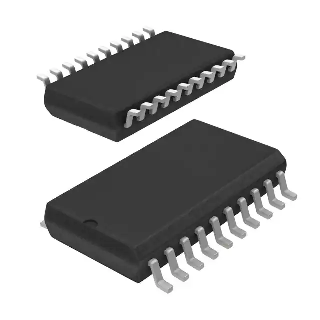
• Packaging (Pb-free & Green available):
– 20-pin 300-mil wide SOIC (S)
– 20-pin 150-mil wide QSOP (Q)
– 20-pin 209-mil wde SSOP (H)
Pericom Semiconductor’s PI49FCT807T and PI49FCT2807T clock
drivers feature one input and ten outputs. The large fanout from a
single input line reduces loading on input clock. TTL level outputs
reduce noise levels on the part. Typical applications are clock and
signal distribution.
Pin Configuration
Block Diagram
A
1
20
VCC
GND
2
19
B9
B0
3
18
B8
4 20-Pin 17
5 H, Q, R16
GND
GND
6
15
VCC
B2
7
8
14
13
B6
VCC
B1
VCC
B3
GND
The PI49FCT2807T also features a 25-ohm on-chip resistor for
lower noise.
B0
B1
B2
B7
B3
B4
GND
9
12
B5
10
11
B4
A
B5
B6
Pin Description
Pin Name
B7
De s cription
A
Input
B0 – B9
Outputs
GND
Ground
VCC
Power
B8
B9
1
PS7008D
09/24/04
�PI49FCT807/2807T
Fast
CMOS
Clock Driver
12345678901234567890123456789012123456789012345678901234567890121234567890123456789012345678901212345678901234567890123456789012123456789012
12345678901234567890123456789012123456789012345678901234567890121234567890123456789012345678901212345678901234567890123456789012123456789012
Maximum Ratings
(Above which the useful life may be impaired. For user guidelines, not tested.)
Storage Temperature ........................................................... –65°C to +150°C
Ambient Temperature with Power Applied ............................ -40°C to +85°C
Supply Voltage to Ground Potential (Inputs & Vcc Only) ..... –0.5V to +7.0V
Supply Voltage to Ground Potential (Outputs & D/O Only) .. –0.5V to +7.0V
DC Input Voltage .................................................................. –0.5V to +7.0V
DC Output Current ............................................................................. 120mA
Note:
Stresses greater than those listed under MAXIMUM RATINGS may cause permanent damage to the device. This is a
stress rating only and functional operation of the device at
these or any other conditions above those indicated in the
operational sections of this specification is not implied.
Exposure to absolute maximum rating conditions for extended periods may affect reliability.
Power Dissipation .................................................................................. 0.5W
DC Electrical Characteristics (Over the Operating Range, TA = –40°C to +85°C, VCC = 5.0V ± 5%)
Test Conditions(1)
Parameters Description
VOH
Output HIGH Voltage
VCC = Min., VIN = VIH or VIL
VOL
Output LOW Current
VCC = Min., VIN = VIH or VIL
VIH
Input HIGH Voltage
Guaranteed Logic HIGH Level
VIL
Input LOW Voltage
Guaranteed Logic LOW Level
IIH
Input HIGH Current
VCC = Max.
IIL
Input LOW Current
VCC = Max.
II
Input HIGH Current
VCC = Max., VIN =VCC (Max.)
VIK
Clamp Diode Voltage
VCC = Min., IIN = –18mA
IOS
Short Circuit Current
VCC = Max.(3), VOUT = GND
IOFF
Power Down Disable
VCC= GND, VOUT = 4.5V
VH
Input Hysteresis
IOH = –15.0mA
IOH = 48.0mA
Min.
Typ.(2)
Max.
Units
2.4
3.3
0.2
0.5
V
V
0.2
0.5
V
IOL = 12mA(25Ω)
2.0
V
0.8
V
VIN = 2.7V
1
µA
VIN = 0.5V
–1
µA
20
µA
–0.7
–1.2
V
–60
–120
–225
mA
—
—
100
µA
150
mV
Capacitance (TA = 25°C, f = 1 MHz)
Parameters(4)
Description
Test Conditions
Typ.
Max.
Units
CIN
Input Capacitance
VIN = 0V
6.0
10
pF
COUT
Output Capacitance
VOUT = 0V
8
12
pF
Notes:
1. For Max. or Min. conditions, use appropriate value specified under Electrical Characteristics for the applicable device type.
2. Typical values are at Vcc = 5.0V, +25°C ambient and maximum loading.
3. Not more than one output should be shorted at one time. Duration of the test should not exceed one second.
4. This parameter is determined by device characterization but is not production tested.
2
PS7008D
09/24/04
�PI49FCT807/2807T
Fast CMOS Clock Driver
12345678901234567890123456789012123456789012345678901234567890121234567890123456789012345678901212345678901234567890123456789012123456789012
Power Supply Characteristics
Test Conditions(1)
Parameters Description
Min.
Typ.(2)
Max.
Units
3
30
µA
ICC
Quiescent Power
Supply Current
VCC = Max.
VIN = GND
or Vcc
∆ICC
Supply Current per
Input @ TTL HIGH
VCC = Max.,
VIN = 3.4V(3)
0.5
1.5
mA
ICCD
Supply Current per
Input per MHz(4)
VCC = Max., Outputs Open
50% Duty Cycle,
One Input Toggling
VIN = VCC
VIN = GND
0.4
0.6
mA/
MHz
IC
Total Power Supply
Current(6)
VCC = Max., Outputs Open
fCP = 50 MHZ,
50% Duty Cycle
VIN = VCC
VIN = GND
VIN = 3.4V
VIN = GND
20
30(5)
mA
20.7
33(5)
Notes:
1. For Max. or Min. conditions, use appropriate value specified under Electrical Characteristics for the applicable device.
2. Typical values are at Vcc = 5.0V, +25°C ambient.
3. Per TTL driven input (VIN = 3.4V); all other inputs at Vcc or GND.
4. This parameter is not directly testable, but is derived for use in Total Power Supply Calculations.
5. Values for these conditions are examples of the Icc formula. These limits are guaranteed but not tested.
6. IC =IQUIESCENT + IINPUTS + IDYNAMIC
IC = ICC + ∆ICC DHNT + ICCD (fCP/2 + fINI)
ICC = Quiescent Current
∆ICC = Power Supply Current for a TTL High Input (VIN = 3.4V)
DH = Duty Cycle for TTL Inputs High
NT = Number of TTL Inputs at DH
ICCD = Dynamic Current Caused by an Input Transition Pair (HLH or LHL)
fCP = Clock Frequency for Register Devices (Zero for Non-Register Devices)
fI = Input Frequency
NI = Number of Inputs at fI
All currents are in milliamps and all frequencies are in megahertz.
Switching Characteristics over Operating Range
Parameters
tPLH
tPHL
t SK(o)
t SK(p)
t SK(t)
Description
Conditions
Propagation Delay
A TO BN
Skew between two outputs
of same package(3)
Skew between opposite
transitions of same
output (|tPHL — tPLH|)(3)
Skew between outputs of
different package at same
power supply, temperature
and speed grade(3)
CL = 50pF
RL = 500Ω
(1)
807/2807T
807AT
807BT
807CT
Com.
Com.
Com.
Com.
Min.
Max.
Min.
Max.
Min.
Max.
Min.
Max. Units
1.5
4.5
1.5
4.0
1.5
3.8
1.5
3.5
ns
—
0.5
—
0.5
—
0.35
—
0.25
ns
—
0.5
—
0.5
—
0.35
—
0.35
ns
—
1.0
—
1.0
—
0.75
—
0.75
ns
Notes:
1. See test circuit and wave forms.
2. Minimum limits are guaranteed but not tested on Propagation Delays.
3. This parameter is guaranteed but not tested.
3
PS7008D
09/24/04
�PI49FCT807/2807T
Fast
CMOS
Clock Driver
12345678901234567890123456789012123456789012345678901234567890121234567890123456789012345678901212345678901234567890123456789012123456789012
12345678901234567890123456789012123456789012345678901234567890121234567890123456789012345678901212345678901234567890123456789012123456789012
Tests Circuits For All Outputs(1)
Switch Position
VCC
7.0V
500Ω
VIN
VOUT
Pulse
Generator
50pF
CL
Switch
Closed
All Other Inputs
Open
Definitions:
CL = Load capacitance: includes jig and probe capacitance.
RT = Termination resistance: should be equal to ZOUT of the Pulse
Generator.
D.U.T.
RT
Test
Open Drain
Disable LOW
Enable LOW
500Ω
Switching Waveforms
Pulse Skew – tSK(p)
Propagation Delay
3V
Input
3V
1.5V
Input
1.5V
0V
0V
tPHL
tPLH
tPLH
VOH
tPHL
VOH
2.0V
Output
1.5V
Output
0.5V
1.5V
VOL
tR
VOL
tF
tSK(p) = tPHL • tPLH
Output Skew – tSK(o)
Package Skew – tSK(t)
3V
Input
1.5V
3V
0V
Input
tPHLx
tPLHx
Ox
1.5V
0V
VOH
tPHL1
tPLH1
1.5V
VOH
Package 1
Output
VOL
tSK(o)
tSK(o)
1.5V
VOL
VOH
Oy
tSK(t)
VOH
1.5V
Package 2
Output
VOL
tPLHy
tSK(t)
1.5V
VOL
tPHLy
tPLH2
tSK(o) = tPLHy • tPLHx or tPHLy • tPHLx
tPHL2
tSK(t) = tPLH2 • tPLH1 or tPHL2 • tPHL1
4
PS7008D
09/24/04
�PI49FCT807/2807T
Fast CMOS Clock Driver
12345678901234567890123456789012123456789012345678901234567890121234567890123456789012345678901212345678901234567890123456789012123456789012
Packaging Mechanical: 20-Pin 209-Mil SSOP (H)
20
.197
.220
5.00
5.60
1
0.09
0.25
.004
.009
.272
.295
6.90
7.50
0.55 .022
0.95 .037
.078
2.00 Max
.291
.322
7.40
8.20
SEATING
PLANE
.002
Min
0.050
.0098
Max.
0.25
.0256
BSC
0.65
X.XX DENOTES DIMENSIONS
X.XX IN MILLIMETERS
Packaging Mechanical: 20-Pin 150-Mil QSOP (Q)
20
.008
0.20
MIN.
.150
.157
.008
.013
0.20
0.33
3.81
3.99
Guage Plane
.010
0.254
1
Detail A
.337 8.56
.344 8.74
.058 REF
1.47
.041
1.04
REF
.015 x 45˚
0.38
.053 1.35
.069 1.75
Detail A
.007
.010
SEATING
PLANE
.016
.050
.025
BSC
0.635
0˚-6˚
.016
.035
0.41
0.89
.004 0.101
.010 0.254
.008 0.203
.012 0.305
0.178
0.254
0.41
1.27
.228
.244
5.79
6.19
X.XX DENOTES DIMENSIONS
X.XX IN MILLIMETERS
5
PS7008D
09/24/04
�PI49FCT807/2807T
Fast
CMOS
Clock Driver
12345678901234567890123456789012123456789012345678901234567890121234567890123456789012345678901212345678901234567890123456789012123456789012
12345678901234567890123456789012123456789012345678901234567890121234567890123456789012345678901212345678901234567890123456789012123456789012
Packaging Mechanical: 20-Pin 300-Mil SOIC (S)
20
.2914
.2992
7.40
7.60
.010
.029
0.254
x 45˚
0.737
1
.496 12.60
.511 12.99
.020 0.508
REF
.030 0.762
.013
.020
0.33
0.51
0.23
0.32
0.41 .016
1.27 .050
.0926
.1043
2.35
2.65
SEATING
PLANE
.050
BSC
1.27
.0091
.0125
0-8˚
.0040
.0118
.394
.419
10.00
10.65
0.10
0.30
X.XX DENOTES CONTROLLING
X.XX DIMENSIONS IN MILLIMETERS
6
PS7008D
09/24/04
�PI49FCT807/2807T
Fast CMOS Clock Driver
12345678901234567890123456789012123456789012345678901234567890121234567890123456789012345678901212345678901234567890123456789012123456789012
Ordering Information
Ordering Code
PI49FCT807TS
PI49FCT807TSE
PI49FCT807TQ
PI49FCT807TQE
PI49FCT807TH
PI49FCT807THE
Package Code
S
S
Q
Q
H
H
Speed Grade
Blank
Blank
Blank
Blank
Blank
Blank
Package Type
20-pin 300-mil SOIC
Pb-free & Green, 20-pin 300-mil SOIC
20-pin 150-mil QSOP
Pb-free & Green, 20-pin 150-mil QSOP
20-pin 209-mil SSOP
Pb-free & Green, 20-pin 209-mil SSOP
PI49FCT807ATS
PI49FCT807ATSE
PI49FCT807ATQ
PI49FCT807ATQE
S
S
Q
Q
A
A
A
A
20-pin 300-mil SOIC
Pb-free & Green, 20-pin 300-mil SOIC
20-pin 150-mil QSOP
Pb-free & Green, 20-pin 150-mil QSOP
PI49FCT807ATH
PI49FCT807ATHE
PI49FCT807BTS
PI49FCT807BTSE
PI49FCT807BTQ
PI49FCT807BTQE
PI49FCT807BTH
PI49FCT807BTHE
PI49FCT807CTS
PI49FCT807CTSE
PI49FCT807CTQ
PI49FCT807CTQE
PI49FCT807CTH
PI49FCT807CTHE
PI49FCT2807TS
PI49FCT2807TSE
PI49FCT2807TQ
PI49FCT2807TQE
PI49FCT2807TH
PI49FCT2807THE
H
H
S
S
Q
Q
H
H
S
S
Q
Q
H
H
S
S
Q
Q
H
H
A
A
B
B
B
B
B
B
C
C
C
C
C
C
Blank
Blank
Blank
Blank
Blank
Blank
20-pin 209-mil SSOP
Pb-free & Green, 20-pin 209-mil SSOP
20-pin 300-mil SOIC
Pb-free & Green, 20-pin 300-mil SOIC
20-pin 150-mil QSOP
Pb-free & Green, 20-pin 150-mil QSOP
20-pin 209-mil SSOP
Pb-free & Green, 20-pin 209-mil SSOP
20-pin 300-mil SOIC
Pb-free & Green, 20-pin 300-mil SOIC
20-pin 150-mil QSOP
Pb-free & Green, 20-pin 150-mil QSOP
20-pin 209-mil SSOP
Pb-free & Green, 20-pin 209-mil SSOP
20-pin 300-mil SOIC
Pb-free & Green, 20-pin 300-mil SOIC
20-pin 150-mil QSOP
Pb-free & Green, 20-pin 150-mil QSOP
20-pin 209-mil SSOP
Pb-free & Green, 20-pin 209-mil SSOP
Notes:
1. Thermal characteristics can be found on the company web site at www.pericom.com/packaging/
Pericom Semiconductor Corporation • 1-800-435-2336 • www.pericom.com
7
PS7008D
09/24/04
�
很抱歉,暂时无法提供与“PI49FCT807ATS”相匹配的价格&库存,您可以联系我们找货
免费人工找货