PI4IOE5V9535
16-bit I2C-bus and SMBus I/O port with interrupt
Features
The PI4IOE5V9535 consists of two 8-bit Configuration
(Input or Output selection), Input, Output and Polarity
Inversion (active HIGH or active LOW operation) registers.
The system master can enable the I/Os as either inputs or
outputs by writing to the I/O configuration bits. The data for
each input or output is kept in the corresponding Input port
or Output port register. The polarity of the read register can
be inverted with the Polarity Inversion register. All registers
can be read by the system master.
The PI4IOE5V9535 is identical to the PI4IOE5V9555 except
for the removal of the internal I/O pull-up resistor which
greatly reduces power consumption when the I/Os are held
LOW.
The PI4IOE5V9535 open-drain interrupt output is activated
when any input state differs from its corresponding Input
Port register state and is used to indicate to the system
master that an input state has changed. The power-on reset
sets the registers to their default values and initializes the
device state machine.
Three hardware pins (A0, A1, A2) vary the fixed I2C-bus
address and allow up to eight devices to share the same I2Cbus/SMBus. The fixed I2C-bus address of the
PI4IOE5V9535 are the same as the PI4IOE5V9535 allowing
up to eight of these devices in any combination to share the
same I2C-bus/SMBus.
Operation power supply voltage from 2.3V to 5.5V
16-bit I/O pins which can be programmed as Input or
Output
5V tolerant I/Os
Polarity inversion register
Active LOW interrupt output
Low current consumption
0Hz to 400KHz clock frequency
Noise filter on SCL/SDA inputs
Power-on reset
ESD protection (4KV HBM and 1KV CDM)
Latch-up tested (exceeds 100mA)
Offered in two different packages: TSSOP-24 and TQFN
4x4-24
Description
The PI4IOE5V9535 is a 24-pin device that provides 16 bits
of General Purpose parallel Input/Output (GPIO) expansion
for I2C-bus/SMBus applications It includes the features such
as higher driving capability, 5V tolerance, lower power
supply, individual I/O configuration, and smaller packaging.
It provides a simple solution when additional I/O is needed
for ACPI power switches, sensors, push buttons, LEDs, fans,
etc.
Pin Configuration
Figure 1: TSSOP-24 ( Top View )
PI4IOE5V9535
Document Number DS40531 Rev 1-2
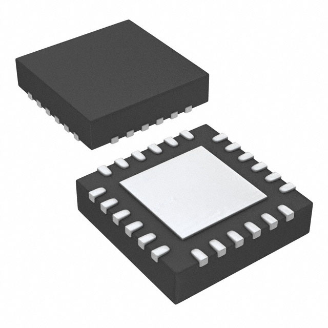
Figure 2: TQFN 4x4-24 ( Top View )
www.diodes.com
1
December 2017
© Diodes Incorporated
�PI4IOE5V9535
Pin Description
Table 1: Pin Description
Pin
TSSOP24
TQFN24
Name
Type
Description
1
22
INT
O
Interrupt input (open-drain)
2
23
A1
I
Address input 1
3
24
A2
I
Address input 2
4
1
IO0_0
I/O
Port 0 input/output 0
5
2
IO0_1
I/O
Port 0 input/output 1
6
3
IO0_2
I/O
Port 0 input/output 2
7
4
IO0_3
I/O
Port 0 input/output 3
8
5
IO0_4
I/O
Port 0 input/output 4
9
6
IO0_5
I/O
Port 0 input/output 5
10
7
IO0_6
I/O
Port 0 input/output 6
11
8
IO0_7
I/O
Port 0 input/output 7
12
9
GND
G
13
10
IO1_0
I/O
Port 1 input/output 0
14
11
IO1_1
I/O
Port 1 input/output 1
15
12
IO1_2
I/O
Port 1 input/output 2
16
13
IO1_3
I/O
Port 1 input/output 3
17
14
IO1_4
I/O
Port 1 input/output 4
18
15
IO1_5
I/O
Port 1 input/output 5
19
16
IO1_6
I/O
Port 1 input/output 6
20
17
IO1_7
I/O
Port 1 input/output 7
21
18
A0
I
Address input 0
22
19
SCL
I
Serial clock line input
23
20
SDA
I
Serial data line open-drain
24
21
VCC
P
Supply voltage
Ground
* I = Input; O = Output; P = Power; G = Ground
PI4IOE5V9535
Document Number DS40531 Rev 1-2
www.diodes.com
2
December 2017
© Diodes Incorporated
�PI4IOE5V9535
Maximum Ratings
Power supply.........................................................................................................-0.5V to +6.0V
Voltage on an I/O pin .............................................................................GND-0.5V to +6.0V
Input current ..........................................................................................................................±20Ma
Output current on an I/O pin ..........................................................................................±50mA
Supply current .....................................................................................................................150mA
Ground supply current ......................................................................................................200mA
Total power dissipation....................................................................................................200mW
Operation temperature...................................................................................................-40~85℃
Storage temperature ................................................................................................... -65~150℃
Maximum Junction temperature ,T j(max) .................................................................. 125℃
Note:
Stresses greater than those listed under MAXIMUM
RATINGS may cause permanent damage to the
device. This is a stress rating only and functional
operation of the device at these or any other
conditions above those indicated in the operational
sections of this specification is not implied.
Exposure to absolute maximum rating conditions
for extended periods may affect reliability.
Static characteristic
VCC = 2.3 V to 5.5 V; GND = 0 V; Tamb= -40 °C to +85 °C; unless otherwise specified.
Table 2: Static characteristic
Symbol
Parameter
Conditions
Min.
Typ.
Max.
Unit
2.3
-
5.5
V
-
40
60
μA
10
20
μA
-
0.25
1
uA
-
0.25
1
uA
-
1.16
1.41
V
Power supply
VCC
Supply voltage
ICC
Supply current
Istb
Standby current
VPOR
Power-on reset voltage
Operating mode; VCC = 5.5 V; no load;
fSCL= 400 kHz
Operating mode; VCC = 2.3 V; no load;
fSCL= 400 kHz
Standby mode; VCC = 5.5 V; no load;
VI = GND; fSCL= 0 kHz; I/O = inputs
Standby mode; VCC = 5.5 V; no load;
VI = VCC; fSCL= 0 kHz; I/O = inputs
[1]
Input SCL, input/output SDA
VIL
Low level input voltage
-0.5
-
+0.3VCC
V
VIH
High level input voltage
0.7VCC
-
5.5
V
IOL
Low level output current
3
-
-
mA
IL
Leakage current
VI=VCC=GND
-1
-
1
μA
Ci
Input capacitance
VI =GND
-
6
10
pF
PI4IOE5V9535
Document Number DS40531 Rev 1-2
VOL=0.4V
www.diodes.com
3
December 2017
© Diodes Incorporated
�PI4IOE5V9535
Static Characteristic Cont.
Symbol
Parameter
Conditions
Min.
Typ.
Max.
Unit
I/Os
VIL
Low level input voltage
-0.5
-
+0.81
V
VIH
High level input voltage
+1.8
-
5.5
V
VCC = 2.3 V to 5.5 V; VOL = 0.5 V[2]
8
10
-
mA
VCC = 2.3 V to 5.5 V; VOL = 0.7 V[2]
10
14
-
mA
IOH=-8mA;VCC=2.3V[3]
1.8
-
-
V
IOH=-10mA;VCC=2.3V[3]
1.7
-
-
V
IOH=-8mA;VCC=3.0V[3]
2.6
-
-
V
IOH=-10mA;VCC=3.0V[3]
2.5
-
-
V
IOH=-8mA;VCC=4.75V[3]
4.1
-
-
V
IOH=-10mA;VCC=4.75V[3]
4.0
-
-
V
VCC=5.5V; VI=VCC
-
-
1
μA
VCC=5.5V; VI=GND
-
-
-1
μA
IOL
VOH
ILIH
ILIL
Low level output current
High level output voltage
High level input leakage
current
Low level input leakage
current
Ci
Input capacitance
-
3.7
10
pF
Co
Output capacitance
-
3.7
10
pF
3
-
-
mA
Interrupt INT
IOL
Low level output current
VOL=0.4V
Select inputs A0,A1,A2
VIL
Low level input voltage
-0.5
-
+0.81
V
VIH
High level input voltage
+1.8
-
5.5
V
1
μA
IL
Input leakage current
-1
Note:
[1]: VCC must be lowered to 0.2 V for at least 20 us in order to reset part.
[2]: Each I/O must be externally limited to a maximum of 25 mA and each octal (IO0_0 to IO0_7 and IO1_0 to IO1_7) must be limited to a maximum current of
100 mA for a device total of 200 mA.
[3]: The total current sourced by all I/Os must be limited to 160 mA.
PI4IOE5V9535
Document Number DS40531 Rev 1-2
www.diodes.com
4
December 2017
© Diodes Incorporated
�PI4IOE5V9535
Dynamic Characteristics
Table 3: Dynamic characteristics
Symbol
Parameter
Standard
mode I2C
Test Conditions
Fast mode I2C
Unit
Min
Max
Min
Max
0
100
0
400
kHz
fSCL
SCL clock frequency
tBUF
bus free time between a STOP and
START condition
4.7
-
1.3
-
μs
tHD;STA
hold time (repeated) START condition
4.0
-
0.6
-
μs
tSU;STA
set-up time for a repeated START
condition
4.7
-
0.6
-
μs
tSU;STO
set-up time for STOP condition
4.0
-
0.6
-
μs
tVD;ACK[1]
data valid acknowledge time
-
3.45
-
0.9
μs
tHD;DAT[2]
data hold time
0
-
0
-
ns
tVD;DAT
data valid time
-
3.45
-
0.9
μs
tSU;DAT
data set-up time
250
-
100
-
ns
tLOW
LOW period of the SCL clock
4.7
-
1.3
-
μs
tHIGH
HIGH period of the SCL clock
4.0
-
0.6
-
μs
tf
fall time of both SDA and SCL signals
-
300
-
300
ns
tr
rise time of both SDA and SCL signals
-
1000
-
300
ns
tSP
pulse width of spikes that must be
suppressed by the input filter
-
50
-
50
ns
Port timing
tv(Q)
Data output valid time[3]
tsu(D)
Data input set-up time
th(D)
Data input hold time
-
200
-
200
ns
150
-
150
-
ns
1
-
1
-
μs
Interrupt timing
tv(INT)
Valid time on pin INT
-
4
-
4
μs
trst(INT)
Reset time on pin INT
-
4
-
4
μs
Note:
[1]: tVD;ACK = time for acknowledgement signal from SCL LOW to SDA (out) LOW.
[2]: tVD;DAT = minimum time for SDA data out to be valid following SCL LOW.
[3]: tv(Q)measured from 0.7VCC on SCL to 50% I/O output.
PI4IOE5V9535
Document Number DS40531 Rev 1-2
www.diodes.com
5
December 2017
© Diodes Incorporated
�PI4IOE5V9535
Figure 3: timing parameters for INT signal
PI4IOE5V9535 Block Diagram
Fig 4: Block diagram
Note: All I/Os are set to inputs at reset.
PI4IOE5V9535
Document Number DS40531 Rev 1-2
www.diodes.com
6
December 2017
© Diodes Incorporated
�PI4IOE5V9535
Details Description
a. Device address
Address Byte
b7(MSB)
b6
b5
b4
b3
b2
b1
b0
0
1
0
0
A2
A1
A0
R/W
Note: Read “1”, Write “0”
b. Registers
i. Command byte
The command byte is the first byte to follow the address byte during a write transmission. It is used as a pointer to determine
which of the following registers will be written or read.
Table 4: Command byte
Command
Register
0
Input port 0
1
Input port 1
2
Output port 0
3
Output port 1
4
Polarity inversion port 0
5
Polarity inversion port 1
6
Configuration port 0
7
Configuration port 1
PI4IOE5V9535
Document Number DS40531 Rev 1-2
www.diodes.com
7
December 2017
© Diodes Incorporated
�PI4IOE5V9535
ii. Register 0 and 1: input port registers
This register is a read-only port. It reflects the incoming logic levels of the pins, regardless of whether the pin is defined as an input
or an output by Register 3. Writes to this register have no effect.
The default value ‘X’ is determined by the externally applied logic level.
Table 5: Input port 0 register
Bit
7
6
5
4
3
2
1
0
Symbol
I0.7
I0.6
I0.5
I0.4
I0.3
I0.2
I0.1
I0.0
Default
X
X
X
X
X
X
X
X
Table 6: Input port 1 register
Bit
Symbol
7
6
5
4
3
2
1
0
I1.7
I1.6
I1.5
I1.4
I1.3
I1.2
I1.1
I1.0
Default
X
X
X
X
X
X
X
X
iii. Register 2 and 3:Output port registers
This register is an output-only port. It reflects the outgoing logic levels of the pins defined as outputs by Registers 6 and 7. Bit
values in this register have no effect on pins defined as inputs. In turn, reads from this register reflect the value that is in the flipflop controlling the output selection, not the actual pin value.
Table 7: Output port 0 register
Bit
7
6
5
4
3
2
1
0
Symbol
O0.7
O0.6
O0.5
O0.4
O0.3
O0.2
O0.1
O0.0
Default
1
1
1
1
1
1
1
1
7
6
5
4
3
2
1
0
Symbol
O1.7
O1.6
O1.5
O1.4
O1.3
O1.2
O1.1
O1.0
Default
1
1
1
1
1
1
1
1
Table 8: Output port 1 register
Bit
iv.
Register 4 and 5: Polarity inversion registers
This register allows the user to invert the polarity of the Input port register data. If a bit in this register is set (written with ‘1’), the
Input port data polarity is inverted. If a bit in this register is cleared (written with a ‘0’), the Input port data polarity is retained.
Table 9: Polarity Inversion port 0 register
Bit
7
6
5
4
3
2
1
0
Symbol
N0.7
N0.6
N0.5
N0.4
N0.3
N0.2
N0.1
N0.0
Default
0
0
0
0
0
0
0
0
PI4IOE5V9535
Document Number DS40531 Rev 1-2
www.diodes.com
8
December 2017
© Diodes Incorporated
�PI4IOE5V9535
Table 10: Polarity Inversion port 1 register
Bit
7
6
5
4
3
2
1
0
Symbol
N1.7
N1.6
N1.5
N1.4
N1.3
N1.2
N1.1
N1.0
Default
0
0
0
0
0
0
0
0
v. Register 6 and 7: Configuration registers
This register configures the directions of the I/O pins. If a bit in this register is set (written with ‘1’), the corresponding port pin is
enabled as an input with high-impedance output driver. If a bit in this register is cleared (written with ‘0’), the corresponding port
pin is enabled as an output. Note that there is a high value resistor tied to VCC at each pin. At reset, the IOs are configured as
inputs with a pull-up to VCC.
Table 11: Configuration port 0 register
Bit
7
6
5
4
3
2
1
0
Symbol
C0.7
C0.6
C0.5
C0.4
C.3
C0.2
C0.1
C0.0
Default
1
1
1
1
1
1
1
1
Table 12: Configuration port 1 register
Bit
7
6
5
4
3
2
1
0
Symbol
C1.7
C1.6
C1.5
C1.4
C1.3
C1.2
C1.1
C1.0
Default
1
1
1
1
1
1
1
1
c. Power-on reset
When power is applied to VCC, an internal power-on reset holds the PI4IOE5V9535 in a reset condition until VCC has reached
VPOR. At that point, the reset condition is released and thePI4IOE5V9535 registers and SMBus state machine will initialize to
their default states. The power-on reset typically completes the reset and enables the part by the time the power supply is above
VPOR. However, when it is required to reset the part by lowering the power supply, it is necessary to lower it below 0.2 V.
d. I/O port
When an I/O is configured as an input, FETs Q1 and Q2 are off, creating a high-impedance. . The input voltage may be raised
above VCC to a maximum of 5.5 V.
If the I/O is configured as an output, then on PI4IOE5V9535 either Q1 or Q2 is on, depending on the state of the Output Port
register. Care should be exercised if an external voltage is applied to an I/O configured as an output because of the low-impedance
path that exists between the pin and either VCC or GND.
PI4IOE5V9535
Document Number DS40531 Rev 1-2
www.diodes.com
9
December 2017
© Diodes Incorporated
�PI4IOE5V9535
Figure 5: Simplified schematic of I/Os
After power-on reset, all registers return to default values.
e. Bus Transaction
i. Writing to the port registers
Data is transmitted to the PI4IOE5V9535 by sending the device address and setting the least significant bit to a logic 0.
The command byte is sent after the address and determines which register will receive the data following the command byte.
The eight registers within the PI4IOE5V9535 are configured to operate as four register pairs. The four pairs are Input Ports,
Output Ports, Polarity Inversion Ports, and Configuration Ports. After sending data to one register, the next data byte will be sent
to the other register in the pair. For example, if the first byte is sent to Output Port 1 (register 3), the next byte will be stored in
Output Port 0 (register 2). There is no limitation on the number of data bytes sent in one write transmission. In this way, each 8bit register may be updated independently of the other registers.
Figure 6: Write to output registers
PI4IOE5V9535
Document Number DS40531 Rev 1-2
www.diodes.com
10
December 2017
© Diodes Incorporated
�PI4IOE5V9535
Write to Output port register
Figure 7: Write to configuration registers
ii. Reading the port registers
In order to read data from the PI4IOE5V9535, the bus master must first send the PI4IOE5V9535 address with the least significant
bit set to a logic 0. The command byte is sent after the address and determines which register will be accessed. After a restart, the
device address is sent again, but this time the least significant bit is set to a logic 1. Data from the register defined by the command
byte will then be sent by the PI4IOE5V9535. Data is clocked into the register on the falling edge of the acknowledge clock pulse.
After the first byte is read, additional bytes may be read but the data will now reflect the information in the other register in the
pair. For example, if you read Input Port 1, then the next byte read would be Input Port 0. There is no limitation on the number of
data bytes received in one read transmission but the final byte received, the bus master must not acknowledge the data.
Figure 8: Read from registers
Note: Transfer can be stopped at any time by a STOP condition.
PI4IOE5V9535
Document Number DS40531 Rev 1-2
www.diodes.com
11
December 2017
© Diodes Incorporated
�PI4IOE5V9535
Figure 9: Read Input port register
Note: Transfer of data can be stopped at any moment by a STOP condition. When this occurs, data present at the latest
acknowledge phase is valid (output mode). It is assumed that the command byte has previously been set to ‘00’ (read Input
Port register).
iii.
Interrupt output
The open-drain interrupt output is activated when one of the port pins changes state and the pin is configured as an input.
The interrupt is deactivated when the input returns to its previous state or the Input Port register is read. A pin configured as an
output cannot cause an interrupt. Since each 8-bit port is read independently, the interrupt caused by Port 0 will not be cleared by
a read of Port 1 or the other way around.
Note: Changing an I/O from an output to an input may cause a false interrupt to occur if the state of the pin does not match
the contents of the Input Port register.
PI4IOE5V9535
Document Number DS40531 Rev 1-2
www.diodes.com
12
December 2017
© Diodes Incorporated
�PI4IOE5V9535
Application Design-In Information
Figure 10: Typical application
Device address configured as 0100 000xb for this example.
IO0_0, IO0_4, IO0_5 configured as outputs.
IO0_1, IO0_2, IO0_3 configured as inputs.
IO0_6, IO0_7, and IO1_0 to IO1_7 configured as inputs.
PI4IOE5V9535
Document Number DS40531 Rev 1-2
www.diodes.com
13
December 2017
© Diodes Incorporated
�PI4IOE5V9535
Minimizing ICC when the I/Os are used to control LEDS
When the I/Os are used to control LEDs, they are normally connected to VCC through a resistor as shown in Figure 11. Since the
LED acts as a diode, when the LED is off the I/O VI is about 1.2 V less than VCC. The supply current, ICC, increases as VI becomes
lower than VCC.
Designs need minimize current consumption, such as battery power applications, should consider maintaining the I/O pins
greater than or equal to VCC when the LED is off. Figure 11 shows a high value resistor in parallel with the LED. Figure 12 shows
VCC less than the LED supply voltage by at least 1.2 V. Both of these methods maintain the I/O VI at or above VCC and prevent
additional supply current consumption when the LED is off.
Figure 11: High value resistor in parallel with the LED
Figure 12: Device supplied by a lower voltage
Part Marking
PI4IOE5V9535
Document Number DS40531 Rev 1-2
www.diodes.com
14
December 2017
© Diodes Incorporated
�PI4IOE5V9535
Packaging Mechanical
TSSOP-24(L)
PI4IOE5V9535
Document Number DS40531 Rev 1-2
www.diodes.com
15
December 2017
© Diodes Incorporated
�PI4IOE5V9535
TQFN-24(ZD)
For latest package info.
please check: http://www.diodes.com/design/support/packaging/pericom-packaging/packaging-mechanicals-and-thermal-characteristics/
Ordering Information
Part Numbers
PI4IOE5V9535LEX
PI4IOE5V9535ZDEX
Package Code
L
ZD
Description
24-Pin, 173mil-Wide (TSSOP)
24-Contact, Very Thin Quad Flat No-Lead (TQFN)
Notes:
Thermal characteristics can be found on the company web site at www.diodes.com/design/support/packaging/
E = Pb-free and Green
X suffix = Tape/Reel
PI4IOE5V9535
Document Number DS40531 Rev 1-2
www.diodes.com
16
December 2017
© Diodes Incorporated
�PI4IOE5V9535
IMPORTANT NOTICE
DIODES INCORPORATED MAKES NO WARRANTY OF ANY KIND, EXPRESS OR IMPLIED, WITH REGARDS TO THIS DOCUMENT, INCLUDING, BUT NOT
LIMITED TO, THE IMPLIED WARRANTIES OF MERCHANTABILITY AND FITNESS FOR A PARTICULAR PURPOSE (AND THEIR EQUIVALENTS UNDER THE
LAWS OF ANY JURISDICTION).
Diodes Incorporated and its subsidiaries reserve the right to make modifications, enhancements, improvements, corrections or other changes without further notice to this
document and any product described herein. Diodes Incorporated does not assume any liability arising out of the application or use of this document or any product
described herein; neither does Diodes Incorporated convey any license under its patent or trademark rights, nor the rights of others. Any Customer or user of this
document or products described herein in such applications shall assume all risks of such use and will agree to hold Diodes Incorporated and all the companies whose
products are represented on Diodes Incorporated website, harmless against all damages.
Diodes Incorporated does not warrant or accept any liability whatsoever in respect of any products purchased through unauthorized sales channel.
Should Customers purchase or use Diodes Incorporated products for any unintended or unauthorized application, Customers shall indemnify and hold Diodes
Incorporated and its representatives harmless against all claims, damages, expenses, and attorney fees arising out of, directly or indirectly, any claim of personal injury or
death associated with such unintended or unauthorized application.
Products described herein may be covered by one or more United States, international or foreign patents pending. Product names and markings noted herein may also
be covered by one or more United States, international or foreign trademarks.
This document is written in English but may be translated into multiple languages for reference. Only the English version of this document is the final and determinative
format released by Diodes Incorporated.
LIFE SUPPORT
Diodes Incorporated products are specifically not authorized for use as critical components in life support devices or systems without the express written approval of the
Chief Executive Officer of Diodes Incorporated. As used herein:
A. Life support devices or systems are devices or systems which:
1. are intended to implant into the body, or
2. support or sustain life and whose failure to perform when properly used in accordance with instructions for use provided in the labeling can be reasonably expected to
result in significant injury to the user.
B. A critical component is any component in a life support device or system whose failure to perform can be reasonably expected to cause the
failure of the life support device or to affect its safety or effectiveness.
Customers represent that they have all necessary expertise in the safety and regulatory ramifications of their life support devices or systems, and acknowledge and
agree that they are solely responsible for all legal, regulatory and safety-related requirements concerning their products and any use of Diodes Incorporated products in
such safety-critical, life support devices or systems, notwithstanding any devices- or systems-related information or support that may be provided by Diodes Incorporated.
Further, Customers must fully indemnify Diodes Incorporated and its representatives against any damages arising out of the use of Diodes Incorporated products in such
safety-critical, life support devices or systems.
Copyright © 2016, Diodes Incorporated
www.diodes.com
PI4IOE5V9535
Document Number DS40531 Rev 1-2
www.diodes.com
17
December 2017
© Diodes Incorporated
�


 工商网监
湘ICP备2023018690号
工商网监
湘ICP备2023018690号
