PI4IOE5V96248
48-bit I2C-bus I/O Expander
Features
Description
Operation power supply voltage from 2.3V to 5.5V
The PI4IOE5V96248 provides general purpose remote I/O
expansion for most microcontroller families via the two-line
bidirectional bus (I2C-bus) and is a part of the Fast-mode Plus
family.
The PI4IOE5V96248 supports high I2C-bus drive (25 mA) so
that many more devices can be on the bus without the need
for bus buffers, high total package sink capacity (1200 mA)
that supports having all 25 mA LEDs on at the same time and
more device addresses (64) are available to allow many more
devices on the bus without address conflicts.
The device consists of a 48-bit quasi-bidirectional port and an
I2C-bus interface. The PI4IOE5V96248 has a low current
consumption and includes latched outputs with high current
drive capability for directly driving LEDs.
It also possesses an interrupt line (INT) which can be
connected to the interrupt logic of the microcontroller. By
sending an interrupt signal on this line, the remote I/O can
inform the microcontroller if there is incoming data on its
ports without having to communicate via the I2C-bus. The
internal Power-On Reset (POR) or software reset sequence
initializes the I/Os as inputs.
48-bit remote I/O pins that default to inputs at power-up
1MHz I2C-bus interface
Compliant with the I2C-bus Fast and Standard modes
5.0V tolerant I/Os
SDA with 30 mA sink capability for 4000 pF buses
Latched outputs with 25 mA sink capability for directly
driving LEDs
Total package sink capability of 1200 mA
Active LOW open-drain interrupt output
Low standby current
64 programmable slave addresses using 3 address pins
ESD protection (4KV HBM and 1KV CDM)
Latch-up tested (exceeds 100mA)
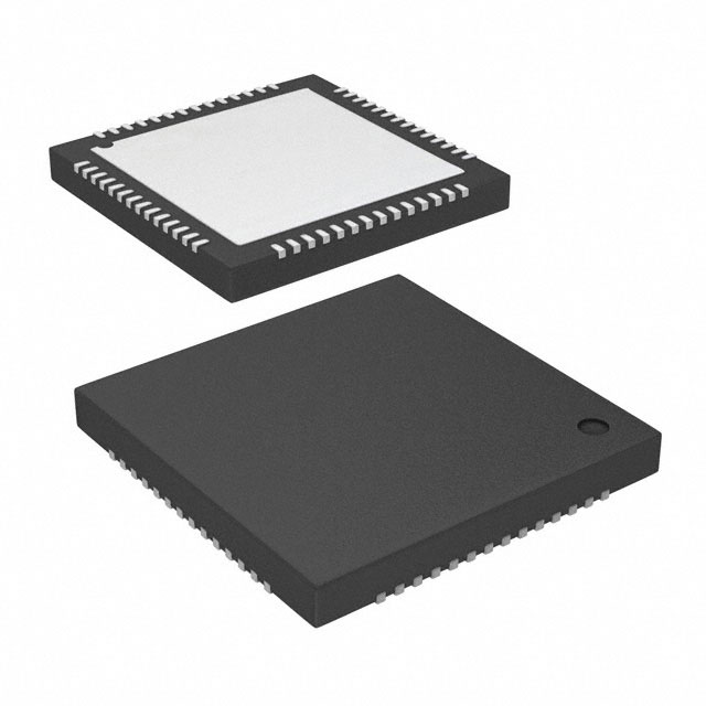
Offered in TQFN-56 7mm x 7mm( ZL 56) package.
PI4IOE5V96248
Document Number DS40436 Rev 1-2
www.diodes.com
1
January 2018
© Diodes Incorporated
�PI4IOE5V96248
Pin Configuration
Fig 1 Pin Assignment of ZL 56
PI4IOE5V96248
Document Number DS40436 Rev 1-2
www.diodes.com
2
January 2018
© Diodes Incorporated
�PI4IOE5V96248
Pin Description
Table 1: Pin Description
Pin
Name
Type
Description
54-56, 1 - 5
IO0_0 - IO0_7
I/O
Port 0 input/output 0 - 7
6 - 13
IO1_0 - IO1_7
I/O
Port 1 input/output 0 - 7
14 - 21
IO2_0 - IO2_7
I/O
Port 2 input/output 0 - 7
22 - 29
IO3_0 - IO3_7
I/O
Port 3 input/output 0 - 7
30 - 37
IO4_0 IO4_7
I/O
Port 4 input/output 0 - 7
38 - 45
IO5_0 - IO5_7
I/O
Port 5 input/output 0 - 7
46
INT
O
Interrupt output (open-drain)
47
SCL
I
Serial clock line input
48
SDA
I
Serial data line open-drain
49
VCC
P
Supply voltage
50
AD0
I
Address input 0
51
AD1
I
Address input 1
52
AD2
I
Address input 2
53
RESET
I
RESET
Thermal Pad
GND
G
Ground
* I = Input; O = Output; P = Power; G = Ground
PI4IOE5V96248
Document Number DS40436 Rev 1-2
www.diodes.com
3
January 2018
© Diodes Incorporated
�PI4IOE5V96248
Maximum Ratings
Power supply.........................................................................................................-0.5V to +6.0V
Voltage on an I/O pin .............................................................................GND-0.5V to +6.0V
Input current .........................................................................................................................±20mA
Output current on an I/O pin ..........................................................................................±50mA
Supply current .................................................................................................................. ±160mA
Ground supply current ....................................................................................................1500mA
Total power dissipation....................................................................................................600mW
Operation temperature...................................................................................................-40~85℃
Storage temperature ................................................................................................... -65~150℃
Maximum Junction temperature ,T j(max) .................................................................. 125℃
Note:
Stresses greater than those listed under MAXIMUM
RATINGS may cause permanent damage to the
device. This is a stress rating only and functional
operation of the device at these or any other
conditions above those indicated in the operational
sections of this specification is not implied.
Exposure to absolute maximum rating conditions
for extended periods may affect reliability.
Static Characteristics
VCC = 2.3 V to 5.5 V; GND = 0 V; Tamb= -40 °C to +85 °C; unless otherwise specified.
Table 2: Static characteristics
Symbol
Parameter
Conditions
Min.
Typ.
Max.
Unit
2.3
-
5.5
V
-
250
500
μA
-
0.25
1
uA
-
1.16
1.41
V
Power supply
VCC
Supply voltage
ICC
Supply current
Istb
Standby current
VPOR
Power-on reset voltage
Operating mode; VCC= 5.5 V; no load;
fSCL= 1MHz
Standby mode; VCC= 5.5 V; no load;
VI = VCC; fSCL= 0 kHz; I/O = inputs
[1]
Input SCL, input/output SDA
VIL
Low level input voltage
-0.5
-
+0.3VCC
V
VIH
High level input voltage
0.7VCC
-
5.5
V
IOL
Low level output current
VOL=0.4V
20
-
-
mA
IL
Leakage current
VI=VCC=GND
-1
-
1
μA
Ci
Input capacitance
VI =GND
-
5
10
pF
VCC = 2.3 V; VOL = 0.5 V[2]
12
28
mA
VCC=3.0V; VOL = 0.5 V[2]
17
35
mA
VCC=4.5V; VOL = 0.5 V[2]
25
42
mA
I/Os
IOL
IOL(tot)
IOH
Itrt(pu)
Low level output current
total LOW-level output
current
VOL=0.5V;VCC=4.5V
HIGH-level output current
VOH = GND
-30
-359
transient boosted pull-up
current
VOH= GND
-0.5
-1.0
600
mA
-480
uA
mA
Ci
Off-state Input capacitance
[3]
-
9
10
pF
Co
Off-state Output capacitance
[3]
-
9
10
pF
PI4IOE5V96248
Document Number DS40436 Rev 1-2
www.diodes.com
4
January 2018
© Diodes Incorporated
�PI4IOE5V96248
Symbol
Parameter
Conditions
Min.
Typ.
Max.
Unit
6
-
-
mA
2.1
10
pF
Interrupt INT
IOL
Low level output current
Co
Output capacitance
VOL=0.4V
Select inputs AD2,AD1,AD0 and RESET
VIL
Low level input voltage
-0.5
-
+0.81
V
VIH
High level input voltage
+1.8
-
5.5
V
1
μA
10
pF
IL
Input leakage current
Ci
input capacitance
-1
2.4
Note:
[1]:VCC must be lowered to 0.2 V for at least 20us in order to reset part.
[2]:Each I/O must be externally limited to a maximum of 25 mA and the total package limited to 1200 mA due to internal busing limits.
[3]: The value is not tested, but verified on sampling basis.
Dynamic Characteristics
Table 3: Dynamic characteristics
Symbol
fSCL
tBUF
tHD;STA
tSU;STA
tSU;STO
Parameter
SCL clock frequency
bus free time between a STOP and
START condition
hold time (repeated) START
condition
set-up time for a repeated START
condition
set-up time for STOP condition
Standard mode
I2C
Fast mode I2C
Fast mode Plus I2C
Unit
Min
Max
Min
Max
Min
Max
0
100
0
400
0
1000
4.7
-
1.3
-
0.5
μs
4.0
-
0.6
-
0.26
μs
4.7
-
0.6
-
0.26
μs
4.0
-
0.6
-
0.26
μs
kHz
tVD;ACK[1]
data valid acknowledge time
-
3.45
-
0.9
-
tHD;DAT[2]
data hold time
0
-
0
-
0
tVD;DAT
data valid time
-
3.45
-
0.9
-
tSU;DAT
data set-up time
250
-
100
-
50
ns
tLOW
LOW period of the SCL clock
4.7
-
1.3
-
0.5
μs
tHIGH
HIGH period of the SCL clock
4.0
-
0.6
-
0.26
μs
-
300
300
-
120
ns
-
1000
300
-
120
ns
-
50
50
50
ns
200
200
ns
tf
tr
tSP
fall time of both SDA and SCL
signals
rise time of both SDA and SCL
signals
pulse width of spikes that must be
suppressed by the input filter
-
0.45
μs
ns
0.45
ns
Port timing CL≤100pF
tv(Q)
Data output valid time[3]
tsu(D)
Data input set-up time
PI4IOE5V96248
Document Number DS40436 Rev 1-2
200
0
0
www.diodes.com
5
0
ns
January 2018
© Diodes Incorporated
�PI4IOE5V96248
Symbol
Parameter
Standard mode
I2C
Min
th(D)
Data input hold time
Max
4
Fast mode I2C
Min
Max
4
Fast mode Plus I2C
Min
Unit
Max
4
μs
Interrupt timing CL≤100pF
tv(D)
Valid time on pin INT
-
4
-
4
-
4
μs
td(rst)
Reset time on pin INT
-
4
-
4
-
4
μs
tw(rst)
Reset pulse width
-
25
-
25
-
25
ns
tvrec(rst)
Reset recovery time[4]
-
0
-
0
-
0
ns
trst
Reset time
-
1
-
1
-
1
μs
Reset timing
Note:
[1]: tVD;ACK = time for acknowledgement signal from SCL LOW to SDA (out) LOW.
[2]: tVD;DAT = minimum time for SDA data out to be valid following SCL LOW.
[3]: tv(Q)measured from 0.7VCC on SCL to 50% I/O output.
Fig 2: timing parameters for INT signal
PI4IOE5V96248
Document Number DS40436 Rev 1-2
www.diodes.com
6
January 2018
© Diodes Incorporated
�PI4IOE5V96248
Block Diagram
Fig 3: Block diagram
Note: All I/Os are set to inputs at reset.
Details Description
a.
Device address
Following a START condition, the bus master must send the address of the slave it is accessing and the operation it wants to
perform (read or write). The address of the PI4IOE5V96248 is shown in below. Slave address pins AD2, AD1, and AD0 choose 1 of
64 slave addresses. To conserve power, no internal pull-up resistors are incorporated on AD2, AD1, and AD0. Address values
depending on AD2, AD1, and AD0 can be found in Table 4 “PI4IOE5V96248 address map”.
PI4IOE5V96248 Address
Address Byte
b7(MSB)
b6
b5
b4
b3
b2
b1
b0
A6
A5
A4
A3
A2
A1
A0
R/W
The last bit of the first byte defines the operation to be performed. When set to logic 1 a read is selected, while a logic 0 selects a
write operation.
PI4IOE5V96248
Document Number DS40436 Rev 1-2
www.diodes.com
7
January 2018
© Diodes Incorporated
�PI4IOE5V96248
Table 4 PI4IOE5V96248Address maps
AD2
AD1
AD0
A6
A5
A4
A3
A2
A1
A0
GND
GND
GND
GND
VDD
VDD
VDD
VDD
GND
GND
GND
GND
VDD
VDD
VDD
VDD
GND
GND
GND
GND
VDD
VDD
VDD
VDD
GND
GND
GND
GND
VDD
VDD
VDD
VDD
SCL
SCL
SCL
SCL
SDA
SDA
SDA
SDA
SCL
SCL
SCL
SCL
SDA
SDA
SCL
SCL
SDA
SDA
SCL
SCL
SDA
SDA
SCL
SCL
SDA
SDA
GND
GND
VDD
VDD
GND
GND
VDD
VDD
GND
GND
VDD
VDD
GND
GND
VDD
VDD
SCL
SCL
SDA
SDA
SCL
SCL
SDA
SDA
SCL
SCL
GND
VDD
GND
VDD
GND
VDD
GND
VDD
SCL
SDA
SCL
SDA
SCL
SDA
SCL
SDA
GND
VDD
GND
VDD
GND
VDD
GND
VDD
SCL
SDA
SCL
SDA
SCL
SDA
SCL
SDA
GND
VDD
GND
VDD
GND
VDD
GND
VDD
SCL
SDA
0
0
0
0
0
0
0
0
0
0
0
0
0
0
0
0
0
0
0
0
0
0
0
0
0
0
0
0
0
0
0
0
1
1
1
1
1
1
1
1
1
1
0
0
0
0
0
0
0
0
0
0
0
0
0
0
0
0
1
1
1
1
1
1
1
1
1
1
1
1
1
1
1
1
0
0
0
0
0
0
0
0
0
0
1
1
1
1
1
1
1
1
1
1
1
1
1
1
1
1
0
0
0
0
0
0
0
0
0
0
0
0
0
0
0
0
1
1
1
1
1
1
1
1
1
1
0
0
0
0
0
0
0
0
1
1
1
1
1
1
1
1
0
0
0
0
0
0
0
0
1
1
1
1
1
1
1
1
0
0
0
0
0
0
0
0
1
1
0
0
0
0
1
1
1
1
0
0
0
0
1
1
1
1
0
0
0
0
1
1
1
1
0
0
0
0
1
1
1
1
0
0
0
0
1
1
1
1
0
0
0
0
1
1
0
0
1
1
0
0
1
1
0
0
1
1
0
0
1
1
0
0
1
1
0
0
1
1
0
0
1
1
0
0
1
1
0
0
1
1
0
0
0
1
0
1
0
1
0
1
0
1
0
1
0
1
0
1
0
1
0
1
0
1
0
1
0
1
0
1
0
1
0
1
0
1
0
1
0
1
0
1
0
1
PI4IOE5V96248
Document Number DS40436 Rev 1-2
www.diodes.com
8
Address
(Write)
20h
22h
24h
26h
28h
2Ah
2Ch
2Eh
30h
32h
34h
36h
38h
3Ah
3Ch
3Eh
40h
42h
44h
46h
48h
4Ah
4Ch
4Eh
50h
52h
54h
56h
58h
5Ah
5Ch
5Eh
A0h
A2h
A4h
A6h
A8h
AAh
ACh
AEh
B0h
B2h
Address
(Read)
21h
23h
25h
27h
29h
2Bh
2Dh
2Fh
31h
33h
35h
37h
39h
3Bh
3Dh
3Fh
41h
43h
45h
47h
49h
4Bh
4Dh
4Fh
51h
53h
55h
57h
59h
5Bh
5Dh
5Fh
A1h
A3h
A5h
A7h
A9h
ABh
ADh
AFh
B1h
B3h
January 2018
© Diodes Incorporated
�PI4IOE5V96248
SCL
SCL
SDA
SDA
SDA
SDA
SCL
SCL
SCL
SCL
SDA
SDA
SDA
SDA
SCL
SCL
SCL
SCL
SDA
SDA
SDA
SDA
SDA
SDA
SCL
SCL
SDA
SDA
GND
GND
VDD
VDD
GND
GND
VDD
VDD
GND
GND
VDD
VDD
GND
GND
VDD
VDD
SCL
SDA
SCL
SDA
SCL
SDA
GND
VDD
GND
VDD
GND
VDD
GND
VDD
SCL
SDA
SCL
SDA
SCL
SDA
SCL
SDA
PI4IOE5V96248
Document Number DS40436 Rev 1-2
1
1
1
1
1
1
1
1
1
1
1
1
1
1
1
1
1
1
1
1
1
1
0
0
0
0
0
0
1
1
1
1
1
1
1
1
1
1
1
1
1
1
1
1
1
1
1
1
1
1
0
0
0
0
0
0
0
0
1
1
1
1
1
1
1
1
1
1
1
1
1
1
0
0
0
0
0
0
0
0
0
0
0
0
0
0
0
0
www.diodes.com
9
0
0
1
1
1
1
0
0
0
0
1
1
1
1
0
0
0
0
1
1
1
1
1
1
0
0
1
1
0
0
1
1
0
0
1
1
0
0
1
1
0
0
1
1
0
1
0
1
0
1
0
1
0
1
0
1
0
1
0
1
0
1
0
1
0
1
B4h
B6h
B8h
BAh
BCh
BEh
C0h
C2h
C4h
C6h
C8h
CAh
CCh
CEh
E0h
E2h
E4h
E6h
E8h
EAh
ECh
EEh
B5h
B7h
B9h
BBh
BDh
BFh
C1h
C3h
C5h
C7h
C9h
CBh
CDh
CFh
E1h
E3h
E5h
E7h
E9h
EBh
Edh
EFh
January 2018
© Diodes Incorporated
�PI4IOE5V96248
Quasi-bidirectional I/O Architecture
The PI4IOE5V96248’s 48 ports (see Figure 4) are entirely independent and can be used either as input or output ports. Input data
is transferred from the ports to the microcontroller in the Read mode. Output data is transmitted to the ports in the Write mode.
Every data transmission from the PI4IOE5V96248 must consist of a multiple of six bytes, the first byte will be referred to as IO_7
to IO_0, and the second byte as IO_15 to IO_8. The third will be referred to as P_23 to IO_16, and so on.
This quasi-bidirectional I/O can be used as an input or output without the use of a control signal for data directions. At power-on
the I/Os are HIGH. In this mode only a current source (IOH) to VCC is active. An additional strong pull-up to VCC (Itrt(pu))
allows fast rising edges into heavily loaded outputs. These devices turn on when an output is written HIGH, and are switched off
by the negative edge of SCL. The I/Os should be HIGH before being used as inputs. After power-on, as all the I/Os are set HIGH,
all of them can be used as inputs. Any change in setting of the I/Os as either inputs or outputs can be done with the write mode.
Remark: If a HIGH is applied to an I/O which has been written earlier to LOW, a large current (IOL) will flow to GND.
Fig 4.Simplified schematic diagram of IOX_0 to IOX_7
Writing to the Port (Output Mode)
To write, the master (microcontroller) first addresses the slave device. By setting the last bit of the byte containing the slave address
to logic 0 the Write mode is entered. The PI4IOE5V96248 acknowledges and the master sends the first data byte for IO0_7 to
IO0_0. After the first data byte is acknowledged by the PI4IOE5V96248, the second data byte IO1_7 to IO1_0 is sent by the master.
After the second data byte is acknowledged by the PI4IOE5V96248, the three data byte IO2_7 to IO2_0 is sent by the master and
so on. Once again, the PI4IOE5V96248 acknowledges the receipt of the data. Each 8-bit data is presented on the port lines after it
has been acknowledged by the PI4IOE5V96248.
The number of data bytes that can be sent successively is not limited. After every six bytes, the previous data is overwritten.
…
Fig 5. Write Mode
PI4IOE5V96248
Document Number DS40436 Rev 1-2
www.diodes.com
10
January 2018
© Diodes Incorporated
�PI4IOE5V96248
Reading from a Port (Input Mode)
All ports programmed as input should be set to logic 1. To read, the master (microcontroller) first addresses the slave device after it
receives the interrupt. By setting the last bit of the byte containing the slave address to logic 1 the Read mode is entered.
The data bytes that follow on the SDA are the values on the ports.
If the data on the input port changes faster than the master can read, this data may be lost.Transfer of data can be stopped at any
moment by a STOP condition. When this occurs, data present at the latest acknowledge phase is valid.
Fig 6.Read input port register
Power-on Reset
When power is applied to VCC, an internal Power-On Reset (POR) holds the PI4IOE5V96248 in a reset condition until VCC has
reached VPOR. At that point, the reset condition is released and the PI4IOE5V96248 registers and I2C-bus state machine will
initialize to their default states. Thereafter VCC must be lowered below 0.2 V to reset the device.
Interrupt Output ( INT )
The PI4IOE5V96248 provides an open-drain interrupt (INT) which can be fed to a corresponding input of the microcontroller.
This gives these chips a kind of master function which can initiate an action elsewhere in the system.
An interrupt is generated by any rising or falling edge of the port inputs. After time t(V)D the signal INT is valid.
The interrupt disappears when data on the port is changed to the original setting or data is read from or written to the device
which has generated the interrupt.
In the write mode, the interrupt may become deactivated (HIGH) on the rising edge of the write to port pulse. On the falling edge
of the write to port pulse the interrupt is definitely deactivated (HIGH).
The interrupt is reset in the read mode on the rising edge of the read from port pulse.
During the resetting of the interrupt itself, any changes on the I/Os may not generate an interrupt. After the interrupt is reset any
change in I/Os will be detected and transmitted as an INT.
RESET Input
A reset can be accomplished by holding the RESET pin LOW for a minimum of tw(rst). The PI4IOE5V96248 registers and I2C-bus
state machine will be held in their default state until the RESET input is once again HIGH.
Part Marking
PI4IOE5V96248
Document Number DS40436 Rev 1-2
www.diodes.com
11
January 2018
© Diodes Incorporated
�PI4IOE5V96248
Packaging Mechanical
For latest package info.
please check: http://www.diodes.com/design/support/packaging/pericom-packaging/packaging-mechanicals-and-thermal-characteristics/
Ordering Information
Part Number
PI4IOE5V96248ZLEX
Package Code
ZL
Package
56-Contact, Very Thin Quad Flat No-Lead (TOFN)
Notes:
Thermal characteristics can be found on the company web site at www.diodes.com/design/support/packaging/
E = Pb-free and Green
X suffix = Tape/Reel
PI4IOE5V96248
Document Number DS40436 Rev 1-2
www.diodes.com
12
January 2018
© Diodes Incorporated
�PI4IOE5V96248
IMPORTANT NOTICE
DIODES INCORPORATED MAKES NO WARRANTY OF ANY KIND, EXPRESS OR IMPLIED, WITH REGARDS TO THIS DOCUMENT, INCLUDING, BUT NOT LIMITED
TO, THE IMPLIED WARRANTIES OF MERCHANTABILITY AND FITNESS FOR A PARTICULAR PURPOSE (AND THEIR EQUIVALENTS UNDER THE LAWS OF ANY
JURISDICTION).
Diodes Incorporated and its subsidiaries reserve the right to make modifications, enhancements, improvements, corrections or other changes without further notice to this document and
any product described herein. Diodes Incorporated does not assume any liability arising out of the application or use of this document or any product described herein; neither does Diodes
Incorporated convey any license under its patent or trademark rights, nor the rights of others. Any Customer or user of this document or products described herein in such applications
shall assume all risks of such use and will agree to hold Diodes Incorporated and all the companies whose products are represented on Diodes Incorporated website, harmless against all
damages.
Diodes Incorporated does not warrant or accept any liability whatsoever in respect of any products purchased through unauthorized sales channel.
Should Customers purchase or use Diodes Incorporated products for any unintended or unauthorized application, Customers shall indemnify and hold Diodes Incorporated and its
representatives harmless against all claims, damages, expenses, and attorney fees arising out of, directly or indirectly, any claim of personal injury or death associated with such
unintended or unauthorized application.
Products described herein may be covered by one or more United States, international or foreign patents pending. Product names and markings noted herein may also be covered by one
or more United States, international or foreign trademarks.
This document is written in English but may be translated into multiple languages for reference. Only the English version of this document is the final and determinative format released
by Diodes Incorporated.
LIFE SUPPORT
Diodes Incorporated products are specifically not authorized for use as critical components in life support devices or systems without the express written approval of the Chief Executive
Officer of Diodes Incorporated. As used herein:
A. Life support devices or systems are devices or systems which:
1. are intended to implant into the body, or
2. support or sustain life and whose failure to perform when properly used in accordance with instructions for use provided in the labeling can be reasonably expected to result in
significant injury to the user.
B. A critical component is any component in a life support device or system whose failure to perform can be reasonably expected to cause the
failure of the life support device or to affect its safety or effectiveness.
Customers represent that they have all necessary expertise in the safety and regulatory ramifications of their life support devices or systems, and acknowledge and agree that they are
solely responsible for all legal, regulatory and safety-related requirements concerning their products and any use of Diodes Incorporated products in such safety-critical, life support
devices or systems, notwithstanding any devices- or systems-related information or support that may be provided by Diodes Incorporated. Further, Customers must fully indemnify
Diodes Incorporated and its representatives against any damages arising out of the use of Diodes Incorporated products in such safety-critical, life support devices or systems.
Copyright © 2016, Diodes Incorporated
www.diodes.com
PI4IOE5V96248
Document Number DS40436 Rev 1-2
www.diodes.com
13
January 2018
© Diodes Incorporated
�