A product Line of
Diodes Incorporated
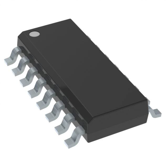
PI5A100
Precision, Wide-Bandwidth Quad SPDT Analog Switch
Description
Features
¼¼ Single Supply Operation (+2V to +6V)
The PI5A100 is an improved Quad Single-pole double-throw
(4SPDT) CMOS analog switch designed to operate with a single
+2V to +6V power supply. The EN pin may be used to place all
switches in a high-impedance state. This high precision device is
ideal for low-distortion audio, video, and data switching and routing.
¼¼ Rail-to-Rail Analog Signal Dynamic Range
¼¼ Low On-Resistance (6Ω typ with 5V supply) Minimizes
Distortion and Error Voltages
¼¼ On-Resistance Matching Between Channels, 0.4Ω Typ.
Each switch conducts current equally well in either direction when
on. In the off state each switch blocks voltages up to the powersupply rails.
¼¼ On-Resistance Flatness, 100mA
¼¼ TTL/CMOS Logic Compatible
¼¼ Low Power Consumption (0.5µW typ.)
Block Diagram/Pin Configuration
¼¼ Packaging (Pb-free & Green Available):
-16-pin SOIC (W)
-16-pin QSOP (Q)
IN 1
Applications
¼¼ Audio, Video Switching and Routing
¼¼ LAN Switches
¼¼ Telecommunication Systems
¼¼ Battery-Powered Systems
Truth Table
EN
0
0
1
PI5A100
IN
0
1
X
Document Number DS40515 Rev 1-2
Decoder
NC1 2
15 EN
NO1 3
14 NC4
COM1 4
13 NO4
NC2 5
12 COM4
NO2 6
11 NC3
COM2 7
10 NO3
GND 8
ON Switch
NC1, NC2, NC3, NC4
NO1, NO2, NO3, NO4
None. Disabled
16 VCC
9
COM3
Notes:
1. Switches shown for logic "0" input.
2. NC = Normally Closed; NO = Normally Open
1
www.diodes.com
December 2017
Diodes Incorporated
�A product Line of
Diodes Incorporated
PI5A100
Absolute Maximum Ratings
Thermal Information
Voltages Referenced to Gnd
VCC.........................................................................-0.5V to +7V
Continuous Power Dissipation
Narrow SOIC & QSOP
(derate 8.7mW/ºC above +70ºC) . . . . . . . . . . . . . . . . . . 650mW
VIN, VCOM, VNC, VNO (1)...............................-0.5V to VCC +2V
..................................................or 30mA, whichever occurs first
Current (any terminal except COM, NO, NC)................... 30mA
Current, COM, NO, NC
(pulsed at 1ms, 10% duty cycle)...................................... 120mA
Storage Temperature . . . . . . . . . . . . . . . . . . . . . -65ºC to +150ºC
Lead Temperature (soldering, 10s). . . . . . . . . . . . . . . . . +300ºC
Notes:
1. Signals on NC, NO, COM, or IN exceeding VCC o.r GND are clamped by internal diodes. Limit forward diode current to 30mA.
2. Caution: Stresses beyond those listed under “Absolute Maximum Ratings” may cause permanent damage to the device. This is a stress
.only rating and operation of the device at these or any other conditions beyond those indicated in the operational sections of this speci fication
is not implied.
Electrical Specifications - Single +5V Supply (VCC = +5V ±10%, GND = 0V, VINH = 2.4V, VINL = 0.8V)
Symbol
Parameter
TestConditions
Temp.
Min.(1)
Full
0
Typ.(2)
Max.(1)
Units
VCC
V
Analog Switch
VANALOG
Analog Switch Range(1)
RON
On-Resistance
∆RON
On-Resistance Match
Between Channels(6)
RFLAT(ON)
On-Resistance Flatness(5)
INO(OFF) or INC(OFF) NO or NC OFF Leakage(6)
25
VCC = 4.5V, ICOM = -30mA,
VNO or VNC = +2.5V
VCC = 5V, ICOM = -30mA,
VNO or VNC = +2.5V
VCC = 5.5C, ICOM = 0V,
VNO or VNC = 4.5V
COM OFF Leakage
Current(6)
VCC = 5.5V, ICOM = 4.5V,
VNO or VNC = ± 4.5V
ICOM(ON)
COM ON Leakage
Current(6)
VCC = 5.5V, ICOM = 4.5V,
VNO or VNC = ± 4.5V
Document Number DS40515 Rev 1-2
Full
10
12
25
0.8
2
Full
ICOM(OFF)
PI5A100
8
2
4
25
2
3
Full
4
25
Full
0.07
-80
25
Full
80
0.01
-80
25
Full
Ω
80
nA
0.016
-80
80
www.diodes.com
December 2017
Diodes Incorporated
�A product Line of
Diodes Incorporated
PI5A100
Electrical Specifications - Single +5V Supply (VCC = +5V ±10%, GND = 0V, VINH = 2.4V, VINL = 0.8V) CONTINUED
Symbol
Parameter
TestConditions
VIH
Input High Voltage
Guaranteed logic High Level
VIL
Input Low Voltage
Guaranteed logic Low Level
IINH
Input Current with Input
Voltage High
VIN = 2.4V, all others = 0.8V
IINL
Input Current with Input
Voltage Low
VIN = 0.8V, all others = 2.4V
Temp.
Min.(1)
Full
2
Typ.(2)
Max.(1)
Units
Logic Input
0.8
Full
-1
0.005
1
-1
0.005
1
8
15
V
µA
Dynamic
tON
25
Turn-On Time
VCC = 5V, See Figure 1
Full
20
25
3.5
tOFF
Turn-Off Time
Q
Charge Injection(3)
CL = 1nF, VGEN = 0V,
RGEN = 0Ω, See Figure 2
OIRR
Off Isolations
RL = 50Ω, CL = 5pF,
f = 10MHz, See Figure 3
-57
XTALK
Crosstalk(8)
RL = 50Ω, CL = 5pF,
f = 10MHz, See Figure 4
-100
C(OFF)
NC or NO Capacitance
f=1kHz, See Figure 5
CCOM(OFF)
COM OFF Capacitance
CCOM(ON)
COM ON Capacitance
f = 1kHz, See Figure 6
BW
-3db Bandwidth
RL = 50Ω See Figure 7
D
Distortion
RL = 10kΩ
7
Full
10
25
10
ns
pC
dB
8
pF
14
18
Full
230
MHz
0.2
%
Supply
VCC
Power-Supply
ICC
Postitive Supply Current
Full
2
VCC = 5.5V, VIN = 0V or
VCC, all channels on or off
6
V
1
µA
Notes:
1. The algebraic convention, where the most negative value is a minimum and the most positive is a maximum, is used in this data sheet.
2. Typical values are for DESIGN AID ONLY, not guaranteed or subject to production testing.
3. Guaranteed by design
4. ΔRΟΝ = RΟΝ max - RΟΝ min
5. Flatness is defined as the difference between the maximum and minimum value of On-Resistance measured.
6. Leakage parameters are 100% tested at maximum rated hot temperature and guaranteed by correlation at +25ºC.
7. Off Isolation = 20log10 [ VCOM / (VNO or VNC) ]. See figure 3.
8. Between any two switches. See figure 4.-
PI5A100
Document Number DS40515 Rev 1-2
3
www.diodes.com
December 2017
Diodes Incorporated
�A product Line of
Diodes Incorporated
PI5A100
Electrical Specifications - Single +3.3V Supply (VCC = +5V ±10%, GND = 0V, VINH = 2.4V, VINL = 0.8V)
Symbol
Parameter
TestConditions
Temp.
Min.(1)
Typ.(2)
Max.(1)
Units
VCC
V
Analog Switch
Analog Switch Range(1)
RON
On-Resistance
∆RON
On-Resistance Match
Between Channels(6)
RFLAT(ON)
On-Resistance Flatness(5)
0
25
VCC = 4.5V, ICOM = -30mA,
VNO or VNC = +2.5V
12
18
Full
25
5
Ω
Full
VCC = 5V, ICOM = -30mA,
VNO or VNC = +2.5V
25
2
4
Full
5
Dynamic
tON
25
Turn-On Time
VCC = 5V, See Figure 1
14
Full
25
tOFF
Turn-Off Time
Q
Charge Injection(3)
CL = 1nF, VGEN = 0V,
RGEN = 0Ω, See Figure 2
25
Postitive Supply Current
VCC = 3.6V, VIN = 0V or
VCC, all channels on or off
Full
25
40
4.5
Full
12
ns
20
5
10
pC
1
µA
Supply
ICC
PI5A100
Document Number DS40515 Rev 1-2
4
www.diodes.com
December 2017
Diodes Incorporated
�A product Line of
Diodes Incorporated
PI5A100
Typical Operating Characteristics (Ta=+25ºC, unless otherwise noted)
RON vs. VCOM
RON vs. VCOM and Temperature
16
40
A: TA = 90°C
B: TA = 25°C
C: TA = -40°C
VCC = +5V
Vcc = +2V
12
RON
RON
30
20
A
8
B
+3.3V
10
+5V
1
2
3
4
VCOM (V)
4
+7V
5
6
0
7
1
0
Leakage Currents vs. Analog Voltage
2
3
5
4
Leakage Current vs. Temperature
10nA
20
VCC = +5V
1nA
16
IA(ON)
)
or IB(ON
)
ON
M(
I CO
100pA
8
IA(ON) or IB(ON)
Leakage
Leakage (pA)
C
0
F)
OF
M(
O
IC
10pA
1pA
-8
0.1pA
-16
0
1
2
3
4
0.01pA
-40
5
0
Temperature (˚C)
80
Crosstalk and Off-Isolation vs. Frequency
Charge Injection vs. Analog Voltage
15
-100
10
Crosstalk
-80
VCC = 5V
-60
5
(dB)
Q-Charge Injection (pC)
40
Temperature (˚C)
Off Isolation
-40
VCC = 3.3V
0
-20
VCC = 5V
-5
0
0
1
2
3
4
5
1
VCOM (V)
PI5A100
Document Number DS40515 Rev 1-2
2
4
6
8 10
20
40
60 80 100
200
Frequency (MHz)
5
www.diodes.com
December 2017
Diodes Incorporated
�A product Line of
Diodes Incorporated
PI5A100
Insertion Loss vs. Frequency
Input Switching Threshold vs. Supply Voltage
0
5
-1
4
-3
-3dB Point
-4
3
VIN, (V)
Insertion Loss (dB)
-2
-5
-6
2
-7
VCC = +5V
R L= 50!
-8
-9
1
0
-10
1
3
30
6 10
Frequency (MHz)
300
60 100
3
RON vs. VCOM and Single Supply
VCC (V)
20
20
tON tOFF (ns)
15
15
10
t ON,
10
tON
5
5
0
7
6
Switching Times vs. Temperature
25
t ON, t OFF (ns)
5
4
tOFF
t OFF
3
3.5
4
4.5
5
5.5
V CC (V)
6
6.5
0
7
-40
0
40
80
120
Temperature (°C)
Supply Current vs. Temperature
10
VCC = +5V
ICC (nA)
1
0.1
0.01
0.001
-40
0
40
80
Temperature (°C)
PI5A100
Document Number DS40515 Rev 1-2
6
www.diodes.com
December 2017
Diodes Incorporated
�A product Line of
Diodes Incorporated
PI5A100
Test Circuits/Timing Diagrams
+5V
Logic +3V
Input
0V
Vcc
Switch
Input +3V*
NO
or NC
COM
RL
100Ohm
IN
Logic
Input
VOUT
tr


 工商网监
湘ICP备2023018690号
工商网监
湘ICP备2023018690号

