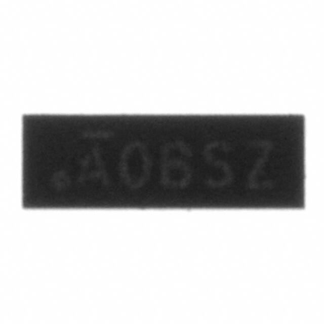
PI5A3158B
Low Voltage Dual SPDT Analog Switch 2:1 Mux/Demux Bus Switch
Features
Description
Application
Pin Assignment
Pin Description
Pin No
8, 11
3, 6
2, 5
1, 4
9, 12
7, 10
Name
1BX
GND
0BX
AX
VCC
SX
Description
Data Port (Normally open)
Ground
Data Port (Normally closed)
Common Output / Data Port
Positive Power Supply
Logic Control
Logic Function Table
Logic Input (SX)
0
1
Function
0BX Connected to AX
1BX Connected to AX
Note: x = 1 or 2
12-pin TDFN
PI5A3158B
Document Number DS41021 Rev 1-2
www.diodes.com
1
June 2018
© Diodes Incorporated
�PI5A3158B
Maximum Ratings
Storage Temperature…………………………………...-65℃ to +150℃
Ambient Temperature with Power Applied......................-40℃ to +85℃
Supply Voltage VCC……………………………………..-0.5V to +7.0V
DC Switch Voltage VIN ………………………………-0.5V to VCC+0.5V
Control Input Voltage VS… ……………………………...-0.5V to +7.0V
DC Output Current VOUT… …………………………………….128mA
DC VCC or Ground Current ICC /IGND… ………………………±100mA
Junction Temperature under Bias (TJ) ......................................... 150°C
Junction Lead Temperature (TL)
(Soldering, 10 seconds) ................................................................ 260°C
Power Dissipation (PD) @ +85°C .............................................. 180mW
ESD(HBM)……………………………….……………….….. 2000V
Note:
Stresses greater than those listed under MAXIMUM
RATINGS may cause permanent damage to the
device. This is a stress rating only and functional
operation of the device at these or any other
conditions above those indicated in the operational
sections of this specification is not implied.
Exposure to absolute maximum rating conditions
for extended periods may affect reliability.
Recommended Operating Conditions
Symbol
VCC
VS
VIN
VOUT
TA
Parameter
Operating Voltage
Control Input Voltage
Switch Input Voltage
Output Voltage
Operating Temperature
Conditions
Control Input VCC = 2.3V - 3.6V
Input Rise and Fall Time
tr, tf
Control Input VCC = 4.5V - 5.5V
Note: Control input must be held HIGH or LOW; it must not float.
PI5A3158B
Document Number DS41021 Rev 1-2
www.diodes.com
2
Min.
1.65
0
0
0
-40
0
0
Typ.
25
-
Max.
5.5
5.5
VCC
VCC
85
10
5
Unit
V
V
V
V
°C
ns/V
ns/V
June 2018
© Diodes Incorporated
�PI5A3158B
DC Electrical Characteristics
(TA = –40°C to 85°C, unless otherwise noted.)
Parameter
Description
Test Conditions
VIAR
Analog Input Signal Range
VCC
VCC=4.5V, IO = 30mA, VIN = 0V
VCC=4.5V, IO=-30mA, VIN =2.4V
VCC=4.5V, IO =-30mA, VIN =4.5V
VCC=4.5V, IO =30mA, VIN = 0V
VCC=4.5V, IO =-30mA, VIN =2.4V
VCC=4.5V, IO =-30mA, VIN =4.5V
VCC=3.0V, IO =24mA, VIN =0V
VCC=3.0V, IO =-24mA, VIN =3.0V
VCC=3.0V, IO =24mA, VIN =0V
VCC=3.0V, IO=-24mA, VIN =3.0V
VCC=2.3V, IO =8mA, VIN =0V
VCC=2.3V, IO =-8mA, VIN =2.3V
VCC=2.3V, IO =8mA, VIN =0V
VCC=2.3V, IO=-8mA, VIN =2.3V
VCC=1.65V, IO =4mA, VIN =0V
VCC=1.65V, IO=-4mA, VIN=1.65V
VCC=1.65V, IO =4mA, VIN = 0V
VCC=1.65V, IO=-4mA, VIN=1.65V
VCC=4.5V, IA=-30mA, VBn=3.15V
VCC=3.0V, IA=-24mA, VBn =2.1V
VCC=2.3V, IA =-8mA, VBn =1.6V
VCC=1.65V, IA=-4mA, VBn=1.15V
VCC=5.0V, IA =-30mA,0≤VBn≤VCC
VCC=3.3V,
IA
=VCC
24mA,0≤VBn
VCC=2.5V, IA =-8mA, 0≤VBn≤VCC
VCC=1.8V, IA =-4mA, 0≤VBn≤VCC
VCC=1.65V
VCC = 2.3V
VCC = 3V
VCC = 4.2V
VCC = 5.5V
VCC=1.65V
VCC = 2.3V
VCC = 3V
VCC = 4.2V
VCC = 5.5V
RON
ON Resistance(1)
∆RON
ON Resistance Match
Between Channels(1,2,3)
RONF
ON Resistance Flatness
(1,2,4)
VIH
Input High Voltage
(Logic High Level)
VIL
Input Low Voltage
(Logic Low Level)
ILKC
Input Leakage Current
0≤VIN≤5.5V, VCC=0V to 5.5V
IOFF
OFF State Leakage
Current
0≤VIN≤5.5V, VCC=1.65V to 5.5V
ICC
Quiescent Supply Current
All channels ON or OFF, VIN = VCC
or GND, IOUT=0, VCC = 5.5V
Temperature
(TA:ºC)
-40°C to 85°C
25°C
-40°C to 85°C
25°C
-40°C to 85°C
25°C
-40°C to 85°C
25°C
-40°C to 85°C
25°C
25°C
-40°C to 85°C
-40°C to 85°C
25°C
-40°C to 85°C
25°C
-40°Cto 85°C
25°C
-40°C to 85°C
Min.
Typ.
Max.
Units
0
-
4
5
7
5
10
6
13
8
20
0.15
0.2
0.3
0.5
6
VCC
6
8
11
6
8
11
8
15
8
15
9
20
9
20
12
30
12
25
-
V
-
12
-
1
1.2
1.3
1.5
1.8
-
22
90
-
0.4
0.6
0.8
1
1.2
±0.1
±1.0
±0.1
±10
1
5
Notes:
1. Measured by voltage drop between A and B pins at the indicated current through the device. ON resistance is determined by the lower of the voltages
on two ports (A or B).
2. Parameter is characterized but not tested in production.
3. DRON = RON max – RON min. measured at identical VCC, temperature and voltage levels.
4. Flatness is defined as difference between maximum and minimum value of ON resistance over the specified range of conditions. Guaranteed by design.
PI5A3158B
Document Number DS41021 Rev 1-2
www.diodes.com
3
June 2018
© Diodes Incorporated
V
V
µA
µA
µA
�PI5A3158B
Capacitance
(1)
(TA = 25°C, unless otherwise noted.)
Symbol
Parameter
CIN
Control Input
CIO-B
For B Port, Switch OFF
Test Conditions
VCC = 5.0V
Min.
-
Typ.
2.5
5.0
Max.
-
-
15.0
-
Units
pF
(1)
CIOA-ON
VCC = 5.0V, f =1 MHz
For A Port, Switch ON
Notes:
1. Capacitance is characterized but not tested in production
Switch and AC Characteristics (1)
Parameter
tPLH
tPHL
tPZL
tPZH
tPLZ
tPHZ
Description
Test Conditions
Propagation
Delay:A to Bn
See test circuit diagrams 1
and 2. V Open (2)
Output Enable Turn
ON Time:
A to Bn
Supply
Voltage
Temperature
Min. Typ. Max. Units
(TA: ºC)
-
0.7
-
-
0.6
-
VCC =4.5V to 5.5V
-
0.4
-
VCC =1.65V to 1.95V
-
9
-
-
5
-
VCC =3.0V to 3.6V
-
3
-
VCC =4.5V to 5.5V
-
2
-
VCC =1.65V to 1.95V
-
9
-
-
6
-
VCC =3.0V to 3.6V
-
5
-
VCC =4.5V to 5.5V
-
3
-
0.5
-
-
0.5
-
-
0.5
-
-
0.5
-
-
-
5
-
-
4
-
-
-63
-
VCC =2.3V to 2.7V
VCC =3.0V to 3.6V
I
See test circuit diagrams 1
& 2.
VI=2VCC for tPZL,
VI=0V for tPZH
VCC =2.3V to 2.7V
See test circuit diagrams 1
and 2.
Output Disable Turn
VI =2VCC for tPLZ,
OFF Time:A to Bn
VI =0V for tPHZ
VCC =2.3V to 2.7V
–40 to 85°C
-40 to 85°C
-40 to 85°C
VCC =1.65V to 1.95V
tBM
Break Before
Make Time
VCC =2.3V to 2.7V
See test circuit diagram 3.
VCC =3.0V to 3.6V
-40 to 85°C
VCC =4.5V to 5.5V
Q
Charge
Injection
OIRR
Off Isolation
CL=0.1nF, VGEN=0V,
RGEN=0
See test circuit 4.
RL=50, VGEN=0V, RGEN
=0, f =10MHz.
See test circuit 5. (3)
VCC = 5.0V
VCC = 3.3V
VCC =1.65V to 5.5V
25°C
25°C
ns
pC
dB
XTALK
Crosstalk Isolation
See test circuit 6. (4)
VCC =1.65V to 5.5V
25°C
-
-64
-
f3dB
–3dB Bandwidth
See test circuit 9
VCC =1.65V to 5.5V
25°C
-
350
-
MHz
Notes:
1. Guaranteed by design.
2. The device contributes no other propagation delay other than the RC delay of the switch ON resistance and the 50pF load capacitance, when driven by an
ideal voltage source with zero output impedance.
3. Off Isolation = 20 Log10 [ VBn/VA ] and is measured in dB.
4. Crosstalk Isolation = 20 Log10 [ VB1/VB0 ] and is measured in dB.
PI5A3158B
Document Number DS41021 Rev 1-2
www.diodes.com
4
June 2018
© Diodes Incorporated
�PI5A3158B
Test Circuits and Timing Diagrams
Note: Input driven by 50ohm source terminated in 500ohm
Note: CL Includes load and stray capacitance
Note: Input PRR=1.0MHz, tW=500nS
S
PI5A3158B
Document Number DS41021 Rev 1-2
www.diodes.com
5
June 2018
© Diodes Incorporated
�PI5A3158B
0V or VIH
0V or VIH
0V or VIH
PI5A3158B
Document Number DS41021 Rev 1-2
www.diodes.com
6
June 2018
© Diodes Incorporated
�PI5A3158B
0V or VIH
Part Marking
ZA Package
PI5A3158B
Document Number DS41021 Rev 1-2
www.diodes.com
7
June 2018
© Diodes Incorporated
�PI5A3158B
Packaging Mechanical
12-TDFN (ZA)
Ordering Information
Part Number
Package Code
PI5A3158BZAEX
ZA
Package
Top Marking
12-Contact, Thin Dual In-Line Flat No-Lead (TDFN)
kE
Notes:
1.
No purposely added lead. Fully EU Directive 2002/95/EC (RoHS), 2011/65/EU (RoHS 2) & 2015/863/EU (RoHS 3) compliant.
2.
See http://www.diodes.com/quality/lead-free/ for more information about Diodes Incorporated’s definitions of Halogen- and Antimony-free, “Green” and
Lead-free.
3.
Thermal characteristics can be found on the company web site at www.diodes.com/design/support/packaging/
4.
E = Pb-free and Green
5.
X suffix = Tape/Reel
PI5A3158B
Document Number DS41021 Rev 1-2
www.diodes.com
8
June 2018
© Diodes Incorporated
�PI5A3158B
IMPORTANT NOTICE
DIODES INCORPORATED MAKES NO WARRANTY OF ANY KIND, EXPRESS OR IMPLIED, WITH REGARDS TO THIS DOCUMENT, INCLUDING, BUT NOT LIMITED
TO, THE IMPLIED WARRANTIES OF MERCHANTABILITY AND FITNESS FOR A PARTICULAR PURPOSE (AND THEIR EQUIVALENTS UNDER THE LAWS OF ANY
JURISDICTION).
Diodes Incorporated and its subsidiaries reserve the right to make modifications, enhancements, improvements, corrections or other changes without further notice to this document and
any product described herein. Diodes Incorporated does not assume any liability arising out of the application or use of this document or any product described herein; neither does
Diodes Incorporated convey any license under its patent or trademark rights, nor the rights of others. Any Customer or user of this document or products described herein in such
applications shall assume all risks of such use and will agree to hold Diodes Incorporated and all the companies whose products are represented on Diodes Incorporated website, harmless
against all damages.
Diodes Incorporated does not warrant or accept any liability whatsoever in respect of any products purchased through unauthorized sales channel.
Should Customers purchase or use Diodes Incorporated products for any unintended or unauthorized application, Customers shall indemnify and hold Diodes Incorporated and its
representatives harmless against all claims, damages, expenses, and attorney fees arising out of, directly or indirectly, any claim of personal injury or death associated with such
unintended or unauthorized application.
Products described herein may be covered by one or more United States, international or foreign patents pending. Product names and markings noted herein may also be covered by one
or more United States, international or foreign trademarks.
This document is written in English but may be translated into multiple languages for reference. Only the English version of this document is the final and determinative format released
by Diodes Incorporated.
LIFE SUPPORT
Diodes Incorporated products are specifically not authorized for use as critical components in life support devices or systems without the express written approval of the Chief Executive
Officer of Diodes Incorporated. As used herein:
A. Life support devices or systems are devices or systems which:
1. are intended to implant into the body, or
2. support or sustain life and whose failure to perform when properly used in accordance with instructions for use provided in the labeling can be reasonably expected to result in
significant injury to the user.
B. A critical component is any component in a life support device or system whose failure to perform can be reasonably expected to cause the
failure of the life support device or to affect its safety or effectiveness.
Customers represent that they have all necessary expertise in the safety and regulatory ramifications of their life support devices or systems, and acknowledge and agree that they are
solely responsible for all legal, regulatory and safety-related requirements concerning their products and any use of Diodes Incorporated products in such safety-critical, life support
devices or systems, notwithstanding any devices- or systems-related information or support that may be provided by Diodes Incorporated. Further, Customers must fully indemnify
Diodes Incorporated and its representatives against any damages arising out of the use of Diodes Incorporated products in such safety-critical, life support devices or systems.
Copyright © 2016, Diodes Incorporated
www.diodes.com
PI5A3158B
Document Number DS41021 Rev 1-2
www.diodes.com
9
June 2018
© Diodes Incorporated
�