PI5C16211
24-Bit Bus Switch
Features
Description
•
•
•
•
Near-Zero propagation delay
5Ω switch connects inputs to outputs
Direct bus connection when switches are ON
Ultra-low quiescent power (0.2 µA typical)
– Ideally suited for notebook applications
• Industrial operating temperature: –40°C to +85°C
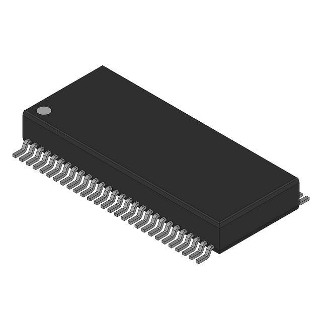
• Packaging (Pb-free & Green available):
– 56-pin 173-mil wide plastic TVSOP
– 56-pin 240-mil wide thin plastic TSSOP
– 56-pin 300-mil wide plastic SSOP
Pericom Semiconductor’s PI5C16211 is a 24-bit bus switch designed
with a low On-Resistance allowing inputs to be connected directly
to outputs. This device operates as a 24-bit or a 12-bit bus switch,
which provides high speed bus switching.
Pin Configuration
Block Diagram
1A1
1B1
1A12
1B12
NC
1
56
1A1
1OE
2
55
1A2
2OE
3
1A3
1 B1
4
54
53
1A4
5
52
1A5
1 B3
6
1A6
1 B4
7
51
50
GND
8
49
GND
1A7
9
48
1A8
1 B6
10
47
1A9
1 B7
46
11
45
12
56-Pin
44
13
1 B8
1A10
1A11
1A12
1OE
2A1
2B1
2A12
2B12
41
VCC
2 B1
17
40
2A3
2 B2
18
39
GND
2 B3
19
20
21
38
37
36
GND
22
23
24
35
34
33
2 B6
25
26
32
31
2 B9
27
28
30
29
2B11
2A7
2A8
2A10
2A11
1A, 1B, I/Os
1A = 1B
1A = 1B
Z
Z
2A, 2B, I/Os
2A = 2B
Z
2A = 2B
Z
2A12
1B12
2 B4
2 B5
2 B7
2 B8
2B10
2B12
Pin Description
Pin Name
xOE
xAx
xBx
Note:
1. H = High Voltage Level, L = Low Voltage Level,
Z = High Impedance
06-0230
1B11
16
2A9
2OE
L
H
L
H
1B10
43
42
2A2
2A6
1OE
L
L
H
H
1 B9
2A1
2A5
Truth Table
1 B5
14
15
2A4
2OE
A, K,V
1 B2
1
I/O
I
I/O
I/O
Description
Output Enables
Bus A
Bus B
PS7050E
07/25/05
�PI5C16211
24-Bit Bus Switch
Maximum Ratings
(Above which the useful life may be impaired. For user guidelines, not tested.)
Storage Temperature .................................................................. –65°C to +150°C
Ambient Temperature with Power Applied ................................. –40°C to +85°C
Supply Voltage to Ground Potential (Inputs & VCC Only)........... –0.5V to +7.0V
Supply Voltage to Ground Potential (Outputs & D/O Only) ........ –0.5V to +7.0V
DC Input Voltage .......................................................................... –0.5V to +7.0V
DC Output Current......................................................................................120mA
Power Dissipation ..........................................................................................1.4W
Note:
Stresses greater than those listed under MAXIMUM
RATINGS may cause permanent damage to the
device. This is a stress rating only and functional
operation of the device at these or any other conditions above those indicated in the operational sections of this specification is not implied. Exposure
to absolute maximum rating conditions for extended
periods may affect reliability.
DC Electrical Characteristics (Over the Operating Range, TA = –40°C to +85°C, VCC = 5V ±10%)
Parameters
VIK
Description
Test Conditions
Clamp Diode Voltage
VCC = 4.5V, II = –18mA
Min.
Typ(1)
Max.
Units
—
1.2
V
VCC = 5.5V, VI = VCC or GND
—
—
10
VCC = 0V, VI = 5.5V
—
—
±1
Quiescent Power Supply Current VCC = 5.5V, VI = VCC or GND
—
—
3.0
ΔICC
Supply Current per Control
Input @ TTL High
—
—
2.5
CI(2)
VCC = 5.5V, One input at 3.4V, other
inputs at VCC or GND
Control Input Capacitance
VI = 3V or 0
—
4.5
CIO
A/B Switch OFF Capacitance
VO = 3V or 0, OE = VCC
—
5.5
II
Input LOW Current
ICC
(OFF)(2)
Switch On Resistance(3)
RON
VCC = 4.0V, VI = 2.4V, II = 15 mA
—
14
20
VCC = 4.5V, VI = 0V, II = 64 mA
—
5
7
VCC = 4.5V, VI = 0V, II = 30 mA
—
5
7
VCC = 4.5V, I = 2.4V, II = 15 mA
—
8
12
µA
mA
PF
Ω
Notes:
1. Typical values are at VCC = 5.0V, TA = 25°C ambient and maximum loading.
2. This parameter is determined by device characterization but is not production tested.
3. Measured by the voltage drop between A and B pin at indicated current through the switch.
ON resistance is determined by the lower of the voltages on the two (A,B) pins.
06-0230
2
PS7050E
07/25/05
�PI5C16211
24-Bit Bus Switch
Power Supply Characteristics
Parameters
Description
Min.
VCC
Supply Voltage
4.0
VIH
High Level Input Voltage
2.0
VIL
Low Level Input voltage
TA
Operating Free-Air Tempertaure
Typ.
Max.
Units
5.5
V
0.8
-40
85
°C
Note:
1. Typical values are at VCC = 5.0V, +25°C ambient.
Switching Characteristics over Operating Range
Parameters
From
(Input)
To
(Output)
tPD(1)
A or B
B or A
tEN
OE
A or B
tDIS
OE
A or B
VCC = 5V ±0.5V
Test
Conditions
Min.
CL = 50pF
RL = 500Ω
Max.
VCC = 4V
Min.
Max.
0.25
0.25
1.5
9.3
10.1
1.5
8.5
7.1
Units
ns
Notes:
1. This parameter is guaranteed but not tested on Propagation Delays. The bus switch contributes no propagational delay other than the RC delay
of the ON resistance of the switch and the load capacitance. The time constant for the switch alone is of the order of 0.25ns for 50pF load. Since
this time constant is much smaller than the rise/fall times of typical driving signals, it adds very little propagational delay to the system. Propagational delay of the bus switch when used in a system is determined by the driving circuit on the driving side of the switch and its interaction
with the load on the driven side.
06-0230
3
PS7050E
07/25/05
�PI5C16211
24-Bit Bus Switch
Packaging Mechanical: 56-pin TVSOP (K)
56
4.30
4.50
.169
.177
0.09
0.20
.0035
.008
1
.441
.449
0.45 .018
0.75 .030
.031
.041
0.80
1.05
11.20
11.40
.252
BSC
6.4
SEATING
PLANE
.016
BSC
0.40
.047
1.20
Max.
.002
.006
0.05
0.15
.005
.009
0.13
0.23
Packaging Mechanical: 56-pin TSSOP (A)
56
.236
.244
1
.547
.555
6.0
6.2
13.9
14.1
1.20
.047
Max.
SEATING PLANE
.004 0.09
.008 0.20
.0197
BSC
0.50
X.XX DENOTES DIMENSIONS
X.XX IN MILLIMETERS
06-0230
.007
.011
0.17
0.27
4
.002
.006
0.05
0.15
0.45 .018
0.75 .030
.319 BSC
8.1
PS7050E
07/25/05
�PI5C16211
24-Bit Bus Switch
Packaging Mechanical: 56-pin SSOP (V)
56
.291
.299
7.39
7.59
.396
.416
10.06
10.56
Gauge Plane
.010 0.25
1
.720 18.29
.730 18.54
.02
.04
0.51
1.01
.015 0.381 x 45˚
.025 0.635
.008
0.20
Nom.
.110 2.79 Max
.025 BSC
0.635
X.XX DENOTES DIMENSIONS
X.XX IN MILLIMETERS
.008
.0135
0.20
0.34
0-8˚
.008 0.20
.016 0.40
Ordering Information
Ordering Code
PI5C16211A
PI5C16211AE
PI5C16211K
PI5C16211KE
PI5C16211V
PI5C16211VE
Package Type
A
A
K
K
V
V
Package Description
56-pin 240-mil wide TSSOP
Pb-free & Green, 56-pin 240-mil wide TSSOP
56-pin 173-mil wide TVSOP
Pb-free & Green, 56-pin 173-mil wide TVSOP
56-pin 300-mil wide SSOP
Pb-free & Green, 56-pin 300-mil wide SSOP
Notes:
1.
2.
Thermal characteristics can be found on the company web site at www.pericom.com/packaging/
For Tape and Reel, include 'x' at the end of the part number.
Pericom Semiconductor Corporation • 1-800-435-2336 • www.pericom.com
06-0230
5
PS7050E
07/25/05
�
很抱歉,暂时无法提供与“PI5C16211AEX”相匹配的价格&库存,您可以联系我们找货
免费人工找货