PI5C3301
12345678901234567890123456789012123456789012345678901234567890121234567890123456789012345678901212345678901234567890123456789012123456789012
12345678901234567890123456789012123456789012345678901234567890121234567890123456789012345678901212345678901234567890123456789012123456789012
SOTiny Single-Bit Bus Switch
TM
Features
Description
• Near-Zero propagation delay
• 5-ohm switches connect inputs to outputs
• Direct bus connection when switches are ON
Pericom Semiconductor’s PI5C3301 is a single digital switch designed
with a fast enable. When enabled using the Bus Enable (BE) pin, the
“A” pin is directly connected to the “B” pin. The bus switch
introduces no additional propagation delay or additional ground
bounce noise.
• Ultra Low Quiescent Power (0.1μA typical)
– Ideally suited for notebook applications
• Packaging (Pb-free & Green available):
– 5-pin plastic SOT23 (T)
– 5-pin plastic SC70 (C)
The PI5C3301 device has an active LOW enable.
Block Diagram
Pin Configuration
A
B
A
1
B
2
GND
3
BE
Truth Table(1)
Vcc
4
BE
Pin Description
BE
A
B
VCC
Function
Pin Name
X*
Hi- Z
Hi- Z
GND
Disconnect
BE
Switch Enable
H
Hi- Z
Hi- Z
VCC
Disconnect
A
Bus A at pin 1
L
B
A
VCC
Connect
B
Bus B at pin 2
Notes:
1. H = High Voltage Level, L = Low Voltage Level
X = Don’t Care, Hi-Z = High Impedance
A = I/O at pin 1, B = I/O at pin 2
* A pull-up resistor should be used for power-up protection
09-0002
5
1
De s cription
VCC
Power
GND
Ground
PS8366I
11/03/08
�PI5C3301
TM
SOTiny Single-Bit Bus Switch
12345678901234567890123456789012123456789012345678901234567890121234567890123456789012345678901212345678901234567890123456789012123456789012
12345678901234567890123456789012123456789012345678901234567890121234567890123456789012345678901212345678901234567890123456789012123456789012
Maximum Ratings
(Above which the useful life may be impaired. For user guidelines, not tested.)
Note:
Stresses greater than those listed under MAXIMUM
RATINGS may cause permanent damage to the device. This
is a stress rating only and functional operation of the device
at these or any other conditions above those indicated in the
operational sections of this specification is not implied.
Exposure to absolute maximum rating conditions for extended periods may affect reliability.
Storage Temperature .......................................................... –65°C to +150°C
Ambient Temperature with Power Applied ..........................–40°C to +85°C
Supply Voltage to Ground Potential ......................................... –0.5V to +7.0V
DC Input Voltage ................................................................... –0.5V to +7.0V
DC Output Current ............................................................................ 120mA
Power Dissipation ................................................................................. 0.5W
DC Electrical Characteristics (Over the Operating Range, TA = –40°C to +85°C, VCC = 5V± 10%)
Parame te rs
Te s t Conditions (1)
De s cription
M in.
Typ.(2)
M ax.
VIH
Input HIGH Voltage
Guaranteed Logic HIGH Level
2 .0
VIL
Input LOW Voltage
Guaranteed Logic LOW Level
–0.5
IIH
Input HIGH Current
VCC = Max., VIN = VCC
±1
IIL
Input LOW Current
VCC = Max., VIN = GND
±1
V
0.8
IOZH
High Impedence Output Current VCC = Max., VOUT = 0V or VCC
±1
IOZL
Low Impedence Output Current VCC = Max., VOUT = 0V or VCC
±1
RON
Switch On
Resistance(3)
Units
VCC = 4.5V, VIN = 0.0V, ION = 30mA or 64mA
VCC = 4.5V, VIN = 2.4V, ION = 15mA
5
10
7
15
VCC = 4V, VIN = 2.4V, ION = 15mA
14
20
μΑ
ohm
Notes:
1. For Max. or Min. conditions, use appropriate value specified under Electrical Characteristics for the applicable device type.
2. Typical values are at VCC = 5.0V, TA = 25°C ambient and maximum loading.
3. Measured by the voltage drop between A and B pin at indicated current through the switch. On-Resistance is determined by the lower of the
voltages on the two (A, B) pins.
Capacitance (TA = 25°C, f = 1 MHz)
Parame te rs (1)
De s cription
CIN
Input Capacitance
C O FF
A/B Capacitance, Switch Off
CON
A/B Capacitance, Switch On
Te s t Conditions
Typ
Units
3
VIN =0V
pF
5
10
Notes:
1. This parameter is determined by device characterization but is not production tested.
09-0002
2
PS8366I
10/29/09
�PI5C3301
TM
SOTiny Single-Bit Bus Switch
12345678901234567890123456789012123456789012345678901234567890121234567890123456789012345678901212345678901234567890123456789012123456789012
12345678901234567890123456789012123456789012345678901234567890121234567890123456789012345678901212345678901234567890123456789012123456789012
Power Supply Characteristics
Parame te rs
Te s t Conditions (1)
De s cription
M in.
ICC
Q uiescent Power Supply Current
VCC = Max.
VIN = GND or VCC
ΔICC
Supply Current per Input @ TTL HIGH
VCC = Max.
VIN = 3.4V(3)
Typ.(2)
M ax.
Units
0.1
3.0
μA
2.5
mA
Notes:
1. For Max. or Min. conditions, use appropriate value specified under Electrical Characteristics for the applicable device.
2. Typical values are at VCC = 5.0V, +25°C ambient.
3. Per TTL driven input (VIN = 3.4V, control inputs only); A and B pins do not contribute to ICC.
Switching Characteristics over Operating Range
PI5C3301
VCC = 4.5V
Parame te rs
De s cription
tPLH
tPHL
Propagation Delay(1,2)
A to B, B to A
tPZH
tPZL
Bus Enable Time
tPHZ
tPLZ
Bus Disable Time
Conditions
C L = 50pF
RL = 500- ohm
M in.
M ax.
VCC = 4V
M in.
M a x.
0.25
0.25
1.0
4.9
5 .5
1.0
4.2
4.5
Units
ns
Notes:
1. This parameter is guaranteed but not tested on Propagation Delays.
2. The bus switch contributes no propagational delay other than the RC delay of the On-Resistance of the switch and the load capacitance. The
time constant for the switch alone is of the order of 0.25ns for 50pF load. Since his time constant is much smaller than the rise/fall times of
typical driving signals, it adds very little propagational delay to the system. Propagational delay of the bus switch when used in a system is
determined by the driving circuit on the driving side of the switch and its interaction with the load on the driven side.
09-0002
3
PS8366I
10/29/09
�TM
PI5C3301
SOTiny Single-Bit Bus Switch
12345678901234567890123456789012123456789012345678901234567890121234567890123456789012345678901212345678901234567890123456789012123456789012
12345678901234567890123456789012123456789012345678901234567890121234567890123456789012345678901212345678901234567890123456789012123456789012
09-0002
4
PS8366I
10/29/09
�PI5C3301
TM
SOTiny Single-Bit Bus Switch
12345678901234567890123456789012123456789012345678901234567890121234567890123456789012345678901212345678901234567890123456789012123456789012
12345678901234567890123456789012123456789012345678901234567890121234567890123456789012345678901212345678901234567890123456789012123456789012
DOCUMENT CONTROL NO.
PD - 1901
REVISION: D
.079 2.00 BSC
.051
1.30
BSC
5
4
DATE: 03/09/05
.083
2.10
BSC
.049
1.25
BSC
1
2
1
.026 0.65
BSC
VIEW A
3
GUAGE PLANE
.006
.011
0.15
0.30
SEATING PLANE
4Û-10Û
.010
.018
0.26
0.46
.321
BSC
0.15
0Û-8Û
.017 0.42 REV
1.10 MAX
SEATING PLANE
0
0
.004 0.10
XXX DENOTES DIMENSIONS
XXX IN MILLIMETERS
Pericom Semiconductor Corporation
3545 N. 1st Street, San Jose, CA 95134
1-800-435-2335 • www.pericom.com
Notes:
1. Controlling dimensions in millimeters
2. Ref: JEDEC MO-203B/AA
3. Package Outline Exclusive of Mold Flash and Metal Burr
DESCRIPTION: 5-Pin, SC70
PACKAGE CODE: C
Note:
• For latest package info, please check: http://www.pericom.com/products/packaging/mechanicals.php
Ordering Information
Ordering Code
Package Code
Package Description
PI5C3301TEX
T
Pb-free & Green, 5-pin SOT23
PI5C3301CEX
C
Pb-free & Green, 5-pin SC70
Notes:
• Thermal characteristics can be found on the company web site at www.pericom.com/packaging/
• E = Pb-free & Green
• X suffix = Tape/Reel
Pericom Semiconductor Corporation • 1-800-435-2336 • www.pericom.com
09-0002
5
PS8366I
10/29/09
�
很抱歉,暂时无法提供与“PI5C3301TEX”相匹配的价格&库存,您可以联系我们找货
免费人工找货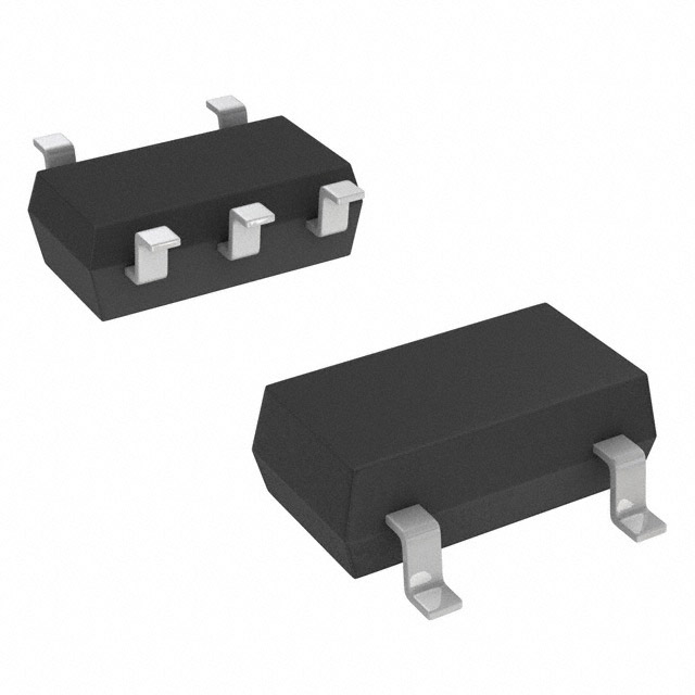


 工商网监
湘ICP备2023018690号
工商网监
湘ICP备2023018690号

