PI5C3384LE

PI5C3384LE

  • 厂商:

    BCDSEMI(美台)

  • 封装:

    TSSOP24

  • 描述:

    IC BUS SWITCH 5 X 1:1 24TSSOP

  • 详情介绍
  • 数据手册
  • 价格&库存
PI5C3384LE 数据手册
PI5C3384 PI5C3384C 10-Bit, 2-Port Bus Switch Features: Description: • Near-Zero propagation delay • 5Ω switches connect inputs to outputs • Direct bus connection when switches are ON • Ultra-low quiescent power (0.2μA typical) – Ideally suited for notebook applications • Packaging (Pb-free & Green Available): – 24-pin 150-mil wide plastic QSOP (Q) – 24-pin 300-mil wide plastic SOIC (S) – 24-pin 173-mil wide plastic TSSOP (L) Pericom Semiconductor’s PI5C3384 and PI5C3384C are 10-bit, 2-port bus switches designed with a low On-Resistance allowing inputs to be connected directly to outputs. The bus switch creates no additional propagational delay or additional ground bounce noise. The switches are turned ON by the Bus Enable (BEx) input signals. Two bus enable signals are provided, one for each of the upper and lower five bits of the two 10-bit buses. Block Diagram Pin Configuration A0 B0 A4 B4 A5 B5 A9 B9 BEA B0 A0 A1 B1 B2 A2 A3 B3 B4 A4 GND 1 2 3 4 5 6 7 8 9 10 11 12 24 23 22 21 20 19 18 17 16 15 14 13 VCC B9 A9 A8 B8 B7 A7 A6 B6 B5 A5 BEB BEA BEB Truth Table(1) Function Disconnect Connect Connect Connect Note: 1. H X L Hi-Z = = = = Pin Description BEA H L H L BEB H H L L B0-B4 Hi-Z A0-A4 Hi-Z A0-A4 Pin Name BEA, BEB A0-A9 B0-A9 GND VCC B5-B9 Hi-Z Hi-Z A5-A9 A5-A9 Description Bus Enable Inputs (Active LOW) Bus A Bus B Ground Power High Voltage Level Don’t Care Low Voltage Level High Impedance 07-0124 1 PS7029F 05/02/07 PI5C3384/3384C 10-Bit, 2-Port Bus switch Maximum Ratings (Above which the useful life may be impaired. For user guidelines, not tested.) Storage Temperature .................................................................. –65°C to +150°C Ambient Temperature with Power Applied ................................. –40°C to +85°C Supply Voltage to Ground Potential (Inputs & VCC Only) ........... –0.5V to +7.0V Supply Voltage to Ground Potential (Outputs & D/O Only) ........ –0.5V to +7.0V DC Input Voltage .......................................................................... –0.5V to +7.0V DC Output Current.....................................................................................120 mA Power Dissipation ..........................................................................................0.5W Note: Stresses greater than those listed under MAXIMUM RATINGS may cause permanent damage to the device. This is a stress rating only and functional operation of the device at these or any other conditions above those indicated in the operational sections of this specification is not implied. Exposure to absolute maximum rating conditions for extended periods may affect reliability. DC Electrical Characteristics (Over the Operating Range, TA = –40°C to +85°C, VCC = 5V ±5%) Parameters Test Conditions(1) Description Min. Typ.(2) Max. VIH Input HIGH Voltage Guaranteed Logic HIGH Level 2.0 VIL Input LOW Voltage Guaranteed Logic LOW Level –0.5 0.8 IIH Input HIGH Current VCC = Max., VIN = VCC –1 1 IIL Input LOW Current VCC = Max., VIN = GND –1 1 IOZ High-Impedance Output Current 0 ≤ A, B ≤ VCC –1 1 VIK Clamp Diode Voltage VCC = Min. IIN = –18 mA IOS Short Circuit Current(3) A (B) = 0V, B (A) = VCC VH Input Hysteresis at Control Pins RON Switch On-Resistance(4) PI5C3384 –0.7 PI5C3384C –1.2 –1.8 100 Units V μA V mA 150 VCC = Min. VIN = 0V ION = 48 mA 5 VCC = Min. VIN = 2.4V ION = 15mA 10 mV 7 Ω 15 Notes: 1. For Max. or Min. conditions, use appropriate value specified under Electrical Characteristics for the applicable device type. 2. Typical values are at VCC = 5.0V, TA = 25°C ambient and maximum loading. 3. Not more than one output should be shorted at one time. Duration of the test should not exceed one second. 4. Measured by the voltage drop between A and B pin at indicated current through the switch. On-Resistance is determined by the lower of the voltages on the two (A,B) pins. 07-0124 2 PS7029F 05/02/07 PI5C3384/3384C 10-Bit, 2-Port Bus switch Capacitance (TA = 25ºC, f = 1 MHz) Parameters(1) CIN Description Test Conditions Typ. Max. Input Capacitance Units 6 COFF A/B Capacitance, Switch Off CON A/B Capacitance, Switch On VIN = 0V 6 pF 8 Notes: 1. This parameter is determined by device characterization but is not production tested. Power Supply Characteristics Parameters ICC ΔICC ICCD Test Conditions(1) Description Typ.(2) Max. PI5C3384 0.1 3.0 PI5C3384C 60 100 Min. Units Quiescent Power Supply Current VCC = Max., VIN = GND or VCC Supply Current per Input @ TTL HIGH VCC = Max., VIN = 3.4V(3) 2.5 mA Supply Current per Input per MHz(4) VCC = Max., A and B Pins Open BE1 or BE2 = GND Control Input Toggling 50% Duty Cycle 0.25 mA/ MHz μA Notes: 1. For Max. or Min. conditions, use appropriate value specified under Electrical Characteristics for the applicable device. 2. Typical values are at VCC = 5.0V, +25°C ambient. 3. Per TTL driven input (VIN = 3.4V, control inputs only); A and B pins do not contribute to ICC. 4. This current applies to the control inputs only and represent the current required to switch internal capacitance at the specified frequency. The A and B inputs generate no significant AC or DC currents as they transition. This parameter is not tested, but is guaranteed by design. Switching Characteristics over Operating Range Parameters Description tPLH tPHL Propagation Delay(2,3) Ax to Bx, Bx to Ax tPZH tPZL Bus Enable Time BEX to Ax or Bx tPHZ tPLZ Bus Disable Time BEx to Ax or Bx Conditions(1) PI5C3384/3384C Min. Typ. Max. Unit 0.25 CL= 50pF RL = 500Ω 1.5 6.5 1.5 5.5 ns Notes: 1. See test circuit and waveforms. 2. This parameter is guaranteed but not tested on Propagation Delays. 3. The bus switch contributes no propagational delay other than the RC delay of the On-Resistance of the switch and the load capacitance. The time constant for the switch alone is of the order of 0.25ns for 50pF load. Since this time constant is much smaller than the rise/fall times of typical driving signals, it adds very little propagational delay to the system. Propagational delay of the bus switch when used in a system is determined by the driving circuit on the driving side of the switch and its interaction with the load on the driven side. 07-0124 3 PS7029F 05/02/07 PI5C3384/3384C 10-Bit, 2-Port Bus switch Switch Position Test Circuit 7V Test Disable LOW Enable LOW tPD VCC Open 500Ω VIN Definitions: CL = Load capacitance (includes jig and probe capacitance) RT = Termination resistance (should be equal to ZOUT of the pulse generator) VOUT Pulse Generator D.U.T. 50pF RT CL Enable and Disable Timing Diagram Enable 500Ω Propagation Delay Diagram Disable 3V 1.5V Control Input 1.5V Same Phase Input Transisiton Output 1.5V 0.3V tPZH 1.5V VOL tPLH 0.3V 0V VOH 1.5V 1.5V VOL tPZH Switch GND tPHL 3V 3V Output Normally High tPLH tPLZ Switch 3V 1.5V 1.5V 0V 0V tPZL Output Normally Low Switch Closed Closed Open tPHL VOH 0V 3V Opposite Phase Input Transisiton 1.5V 0V 1. Input Control Enable = Low; Input Control Disable = High 2. Pulse Generator for all pulses: Rate
PI5C3384LE
物料型号:PI5C3384和PI5C3384C

器件简介: - 这些总线开关设计用于低导通电阻,允许输入直接连接到输出。 - 总线开关不会产生额外的传播延迟或额外的地弹噪声。 - 通过总线使能(BEx)输入信号来打开开关。

引脚分配: - BEA, BEB:总线使能输入(低电平有效) - A0-A9:总线A - B0-B9:总线B - GND:地 - Vcc:电源

参数特性: - 存储温度:-65°C至+150°C - 工作温度:-40°C至+85°C - 供电电压:-0.5V至+7.0V - 输入高电平电压(VIH):最小2.0V - 输入低电平电压(VIL):-0.5V至0.8V - 输入高电平电流(IIH):最大1mA - 输入低电平电流(IL):最大1mA - 高阻态输出电流(IOZ):最大1mA - 钳位二极管电压(VIK):PI5C3384为-0.7V至-1.2V,PI5C3384C为-1.8V - 短路电流(IOS):最大100mA - 输入滞后电压(VH):150mV - 开关导通电阻(RON):在5mA电流下最小值为5欧姆,10mA电流下为7欧姆

功能详解: - 通过BEA和BEB信号来控制总线A和B的连接。 - 断开时,总线端口呈现高阻态。 - 连接时,可以选择连接总线A的0到4位或5到9位,或者总线B的相应位。

应用信息: - 该器件非常适合用于笔记本电脑等应用,因为它具有超低的静态功耗(典型值为0.2μA)。
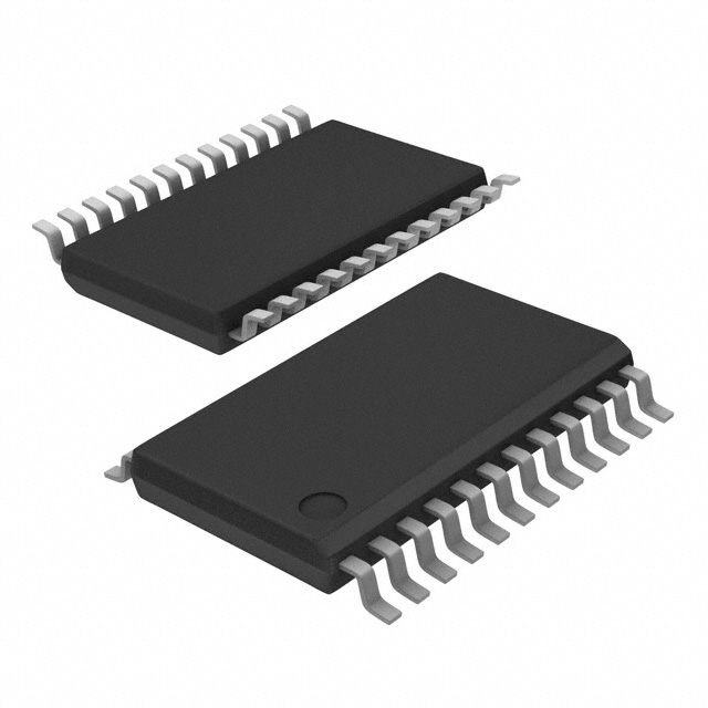
封装信息: - 24引脚150密耳宽塑料QSOP(Q) - 24引脚300密耳宽塑料SOIC(S) - 24引脚173密耳宽塑料TSSOP(L)

订购信息: - PI5C3384L:24引脚173密耳宽塑料TSSOP - PI5C3384LE:无铅和绿色,24引脚173密耳宽塑料TSSOP - PI5C3384Q:24引脚150密耳宽塑料QSOP - PI5C3384QE:无铅和绿色,24引脚150密耳宽塑料QSOP - PI5C3384S:24引脚300密耳宽塑料SOIC - PI5C3384CO:24引脚150密耳宽塑料QSOP - PI5C3384COE:无铅和绿色,24引脚150密耳宽塑料QSOP
PI5C3384LE 价格&库存

很抱歉,暂时无法提供与“PI5C3384LE”相匹配的价格&库存,您可以联系我们找货

免费人工找货